Field-effect transistor, method for manufacturing field-effect transistor, display device using field-effect transistor, and semiconductor device
a field-effect transistor and field-effect technology, applied in the field of field-effect transistors, can solve the problems of difficult to form a crystalline silicon-based thin film on a glass substrate or on a substrate formed of an organic substance, large amount of energy and a large number of steps, and difficulty in reducing the number of masks. the effect of reducing the number of masks
- Summary
- Abstract
- Description
- Claims
- Application Information
AI Technical Summary
Benefits of technology
Problems solved by technology
Method used
Image

Examples
embodiment 1
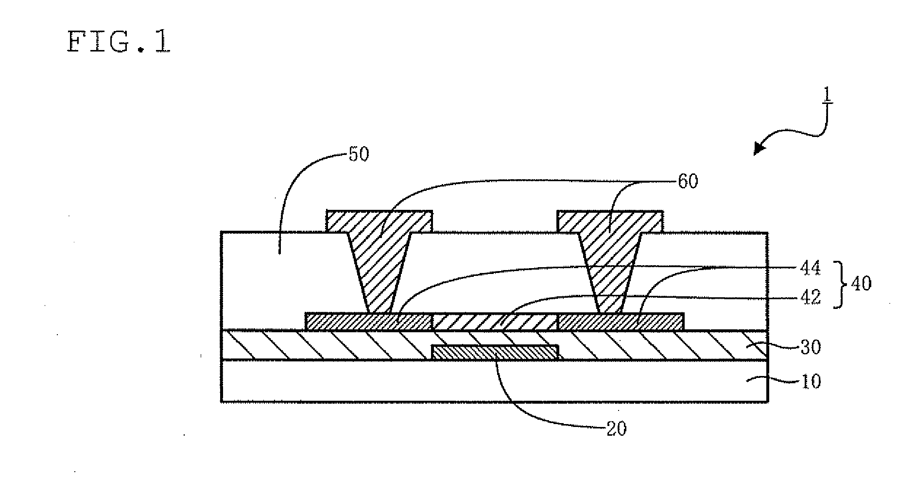
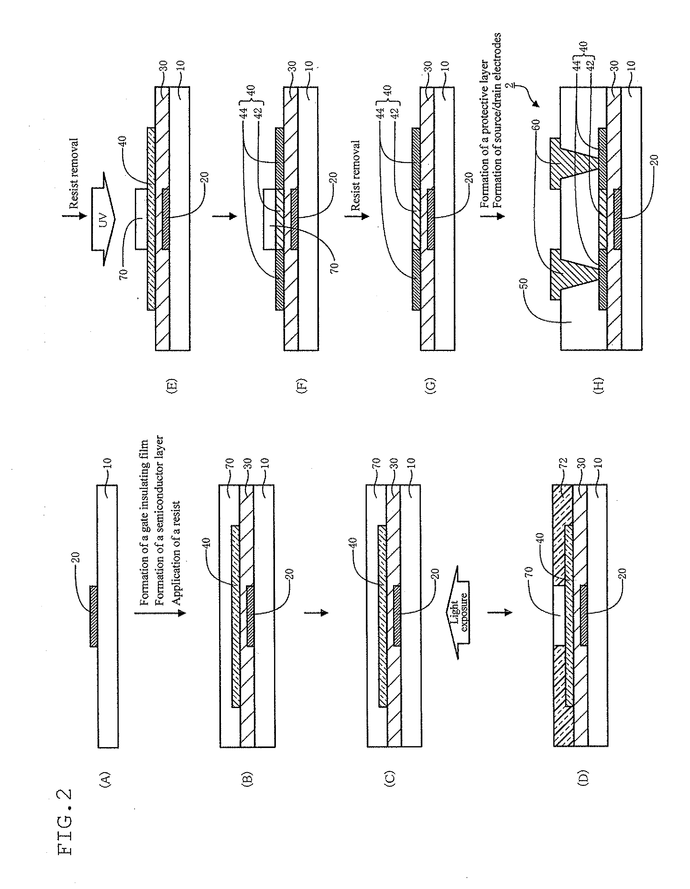
[0167]FIG. 2 is a view showing steps of one embodiment of the method for producing a field effect transistor (bottom-gate type) according to the first aspect of the invention.
[0168]In this embodiment, at first, a gate electrode 20 is formed on a supporting substrate 10 (FIG. 2(A)). A gate insulating film 30 is formed so as to cover the gate electrode 20. On the gate insulating film 30 thus formed, a semiconductor layer 40 and a resist 70 are stacked (FIG. 2(B)). For this stack, light exposure from the direction of the supporting substrate 10 and removal of the resist are conducted, whereby the resist 70 is patterned into a desired shape (FIG. 2(C), FIG. 2(D) and FIG. 2(E)). A resist 72 after the light exposure is removed; and the stack in which the resist 70 has been patterned is then irradiated with UV rays from the direction of the semiconductor layer to reduce the resistance of part of the semiconductor layer, whereby a channel part 42 and source / drain parts 44 are formed in the ...
embodiment 2
[0181]FIG. 3 is a view showing steps of another embodiment of the method for producing a field effect transistor (bottom-gate type) according to the first aspect of the invention.
[0182]In this embodiment, at first, the gate electrode 20 is formed on the supporting substrate 10 (FIG. 3(A)). The gate insulating film 30 is formed so as to cover the gate electrode 20. On the gate insulating film 30 thus formed, the semiconductor layer 40, a protective film 80 and the resist 70 are stacked (FIG. 3(B)). For this stack, light exposure from the direction of the supporting substrate 10 and removal of the resist are conducted, whereby the resist 70 is patterned into a desired shape (FIG. 3(C), FIG. 3(D) and FIG. 3(E)). The protective film of the stack in which the resist 70 has been patterned is etched to pattern the protective film into a desired shape. Then, the patterned resist 70 is removed (FIG. 3(F)). The stack having the patterned protective film 80 on the semiconductor layer 40 is irr...
embodiment 3
[0185]FIG. 4 is a view showing steps of another embodiment of the method for producing a field effect transistor (bottom-gate type) according to the first aspect of the invention.
[0186]In this embodiment, at first, the gate electrode 20 is formed on the supporting substrate 10 (FIG. 4(A)). The gate insulating film 30 is formed so as to cover the gate electrode 20. On the gate insulating film 30 thus formed, the semiconductor layer 40 and the resist 70 are stacked (FIG. 4(B)). For this stack, light exposure from the direction of the supporting substrate 10 and removal of the resist are conducted, whereby the resist 70 is patterned into a desired shape (FIG. 4(C), FIG. 4(D) and FIG. 4(E)). The stack in which the resist 70 has been patterned is subjected to an oxygen plasma treatment from the direction of the semiconductor layer to increase the resistance of part of the semiconductor layer, whereby the channel part 42 and source / drain parts 44 are formed in the semiconductor layer 40 (...
PUM
 Abstract
Description
Claims
Application Information
 - Generate Ideas
- Intellectual Property
- Life Sciences
- Materials
- Tech Scout
- Unparalleled Data Quality
- Higher Quality Content
- 60% Fewer Hallucinations
Browse by: Latest US Patents, China's latest patents, Technical Efficacy Thesaurus, Application Domain, Technology Topic, Popular Technical Reports.
© 2025 PatSnap. All rights reserved.Legal|Privacy policy|Modern Slavery Act Transparency Statement|Sitemap|About US| Contact US: help@patsnap.com