Memory device and semiconductor device

a memory device and semiconductor technology, applied in semiconductor devices, instruments, climate sustainability, etc., can solve the problems of high power consumption of flash memory as a memory device, high power consumption of flash memory, etc., and achieve the effect of increasing the number of rewriting times

Active Publication Date: 2011-06-30
SEMICON ENERGY LAB CO LTD
View PDF99 Cites 111 Cited by
  • Summary
  • Abstract
  • Description
  • Claims
  • Application Information

AI Technical Summary

Benefits of technology

[0025]Furthermore, a memory device in which the number of rewriting times can be increased, and a semiconductor device using the memory device c

Problems solved by technology

Accordingly, power consumption becomes high when a flash memory operates, for example, in data writing and in data erasing, which is one factor that an electronic device including a flash memory as a memory device consumes high power.
In particular, when a flash memory is used for a portable electronic device such as a camera and a mobile phone, high power

Method used


Image

  • Memory device and semiconductor device
  • Memory device and semiconductor device
  • Memory device and semiconductor device

Examples


embodiment 1

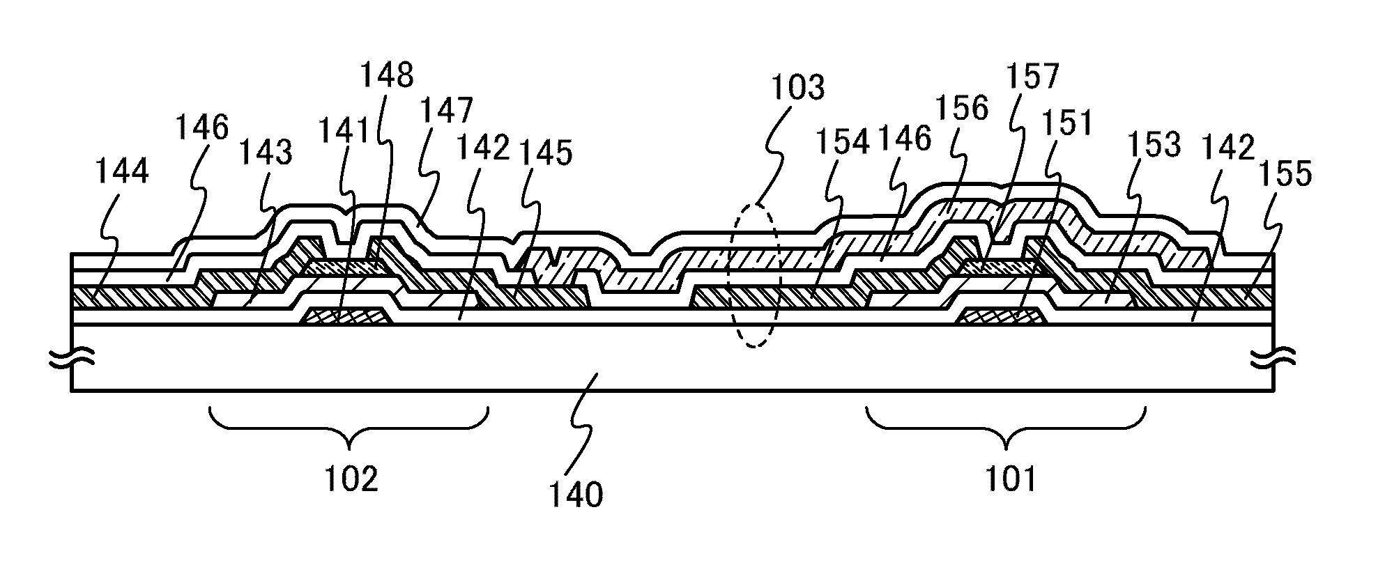
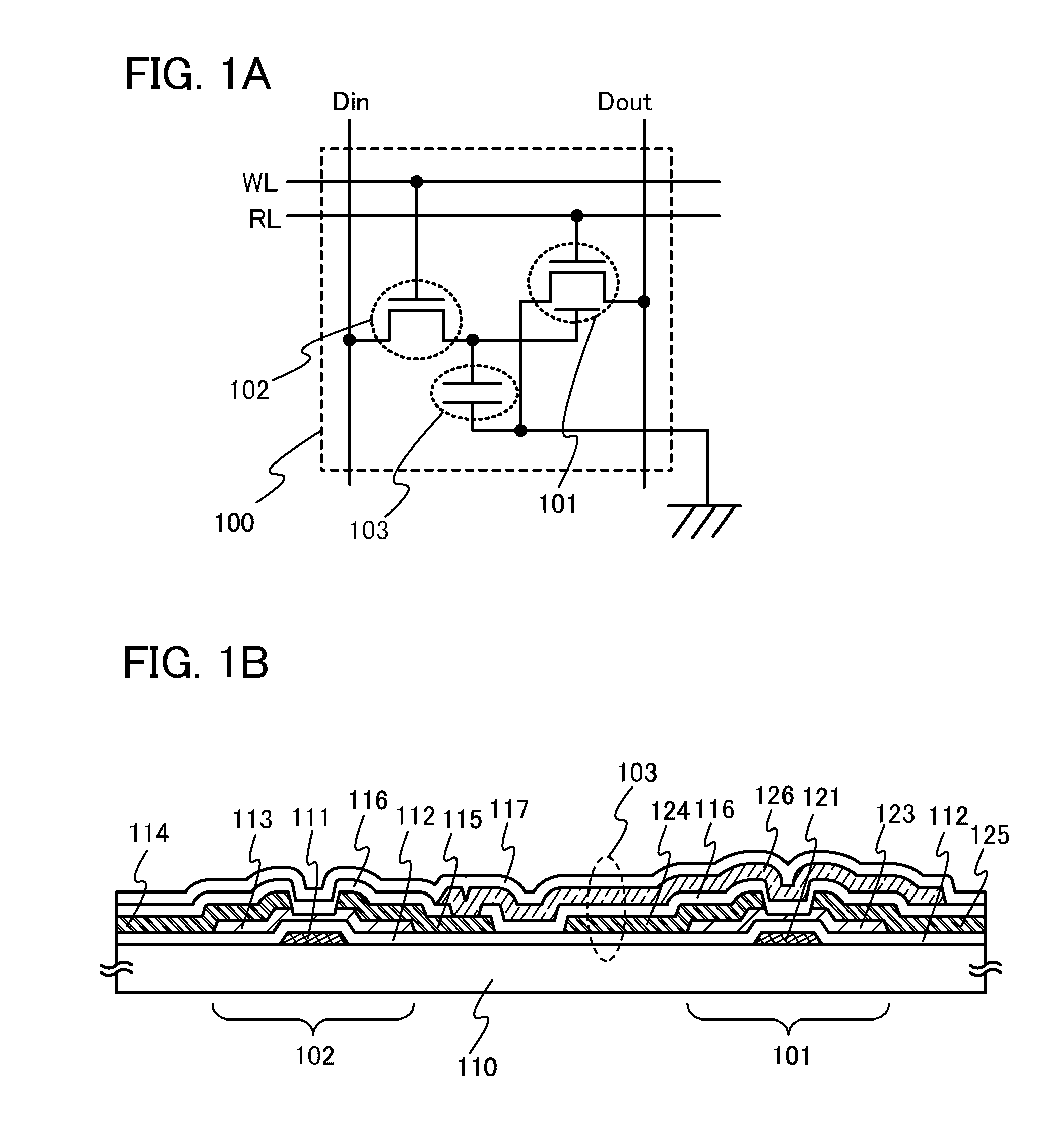
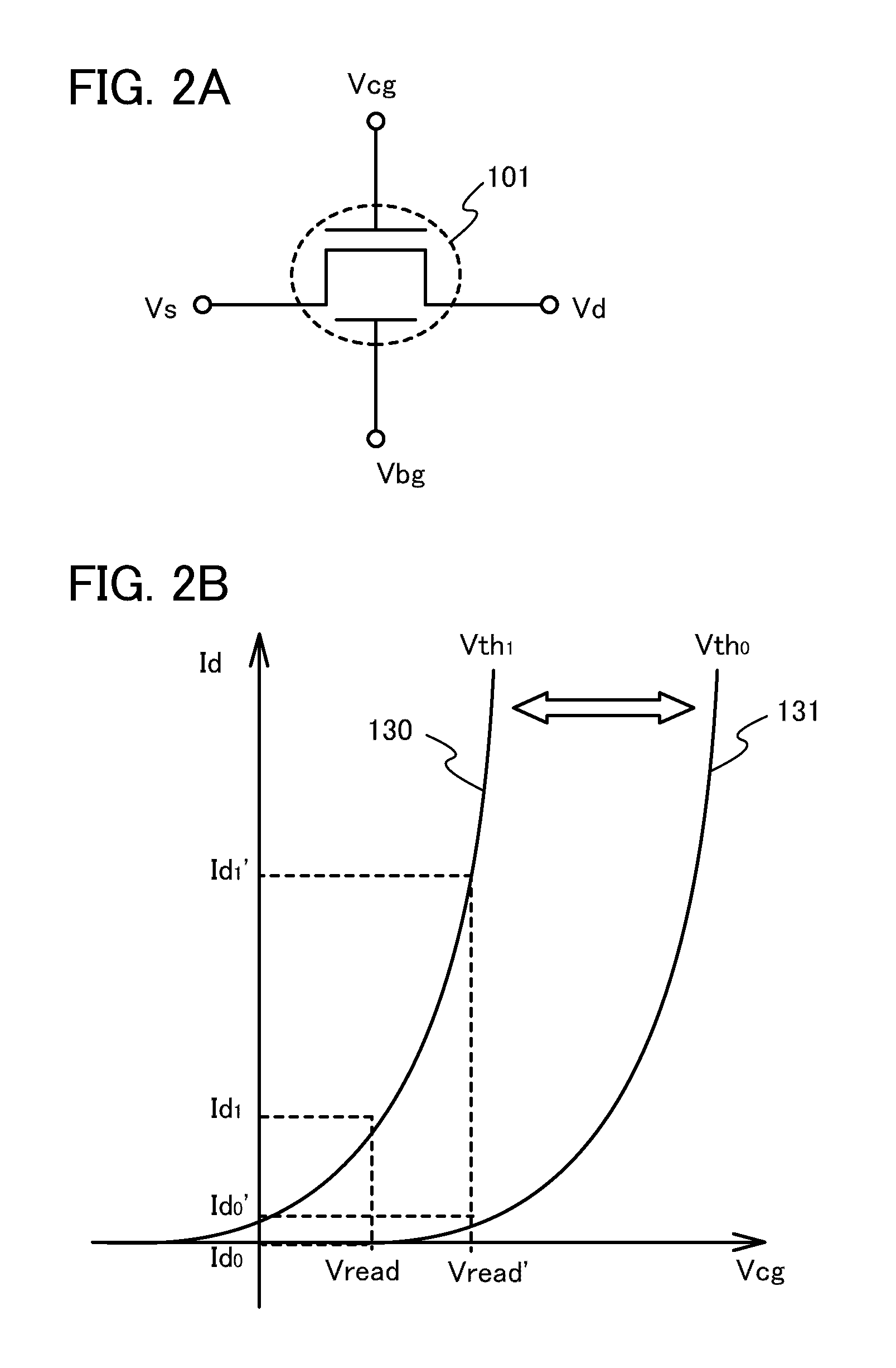
[0049]FIG. 1A illustrates one example of a circuit diagram of a memory cell which is the minimum unit of a memory device of the present invention. A memory cell 100 in FIG. 1A includes a transistor 101 which functions as a memory element and a transistor 102 which can control the supply of a potential to a second gate electrode of the transistor 101 and functions as a switching element. Further, a memory cell may be include a capacitor 103 for holding the potential of the second gate electrode of the transistor 101.

[0050]Note that the memory cell 100 may further have another circuit element such as a diode, a resistor, or an inductor as needed.

[0051]The transistor 101 which functions as a memory element has a first gate electrode, the second gate electrode, a semiconductor film located between the first gate electrode and the second gate electrode, a first insulating film located between the first gate electrode and the semiconductor film, a second insulating film located between th...

embodiment 2

[0106]In Embodiment 2, an example of a structure of a memory device including a plurality of memory cells and a driving method thereof will be described.

[0107]As an example, FIG. 5 illustrates a circuit diagram of a cell array in a NOR-type memory device in which a plurality of memory cells 300 is arranged in matrix. The description of a structure of the memory cell 100 in Embodiment 1 can be referred to for a structure of each memory cell 300 included in the memory device in FIG. 5.

[0108]Specifically, the memory cell 300 includes a transistor 301 which functions as a memory element and a transistor 302 which functions as a switching element, and which can control the supply of a potential to a second gate electrode of the transistor 301. In addition, the memory cell 300 may include a capacitor 303 for holding the potential of the second gate electrode of the transistor 301. The memory cell 300 may further include another circuit element such as a diode, a resistor, or an inductor, ...

embodiment 3

[0170]A channel-etched bottom-gate transistor is given as an example, and a manufacturing method of a memory device according to one embodiment of the present invention will be described. Note that in Embodiment 3, the case where an oxide semiconductor film is used as an active layer in both of a transistor which functions as a memory element and a transistor which functions as a switching element is given as an example for description.

[0171]As illustrated in FIG. 10A, a gate electrode 401 and a gate electrode 402 are formed over a substrate 400 having an insulating surface.

[0172]Although there is no particular limitation on a substrate that can be used as the substrate 400 having an insulating surface, the substrate needs to have heat resistance high enough to withstand at least heat treatment to be performed in a later step. For example, a glass substrate formed by a glass fusion process or a float process can be used. In the case where a glass substrate is used and the temperatur...


PUM


Abstract

It is an object to provide a memory device whose power consumption can be suppressed and a semiconductor device including the memory device. As a switching element for holding electric charge accumulated in a transistor which functions as a memory element, a transistor including an oxide semiconductor film as an active layer is provided for each memory cell in the memory device. The transistor which is used as a memory element has a first gate electrode, a second gate electrode, a semiconductor film located between the first gate electrode and the second gate electrode, a first insulating film located between the first gate electrode and the semiconductor film, a second insulating film located between the second gate electrode and the semiconductor film, and a source electrode and a drain electrode in contact with the semiconductor film.

Description

TECHNICAL FIELD[0001]The present invention relates to a non-volatile semiconductor memory device. In particular, the present invention relates to a structure of a memory cell storing data and a driving method thereof.BACKGROUND ART[0002]Examples of a semiconductor memory device (hereinafter, simply referred to as a memory device) include a DRAM and an SRAM, which are categorized as a volatile memory; a mask ROM, an EPROM, an EEPROM, a flash memory, and a ferroelectric memory, which are categorized as a non-volatile memory; and the like. Most of these memories including single crystal semiconductor substrates are already put into practical use. Among the above semiconductor memories, flash memories are widely marketed, which are mainly used for mobile storage media such as USB memories and memory cards. The reason of this is that flash memories are resistant to physical impact and can be conveniently used because they are non-volatile memories which can repeatedly write and delete da...

Claims


Application Information

Patent Timeline
IPC IPC(8): H01L29/12
CPCG11C16/0433H01L27/115H01L27/13H01L27/1225H01L27/1156H01L29/7869H10B69/00Y02D10/00H10B41/70H10B43/30H10B99/00H01L27/124H01L27/1251H01L27/1255H01L29/78648
Inventor SHIONOIRI, YUTAKAMIYAKE, HIROYUKIKATO, KIYOSHI
Owner SEMICON ENERGY LAB CO LTD
Why Eureka
Try Eureka