High-k metal gate electrode structures formed at different process stages of a semiconductor device

US20110156154A1Active Publication Date: 2011-06-30GLOBALFOUNDRIES US INC

Image

  • High-k metal gate electrode structures formed at different process stages of a semiconductor device
  • High-k metal gate electrode structures formed at different process stages of a semiconductor device
  • High-k metal gate electrode structures formed at different process stages of a semiconductor device

Examples


Embodiment Construction

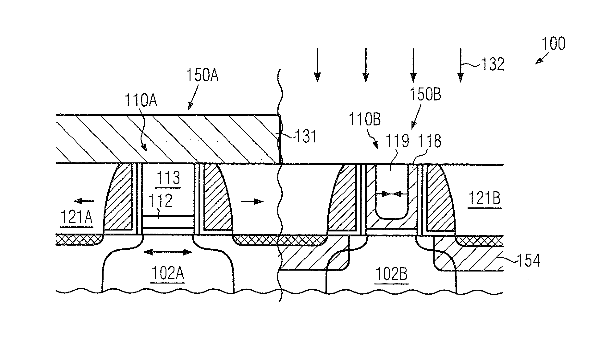
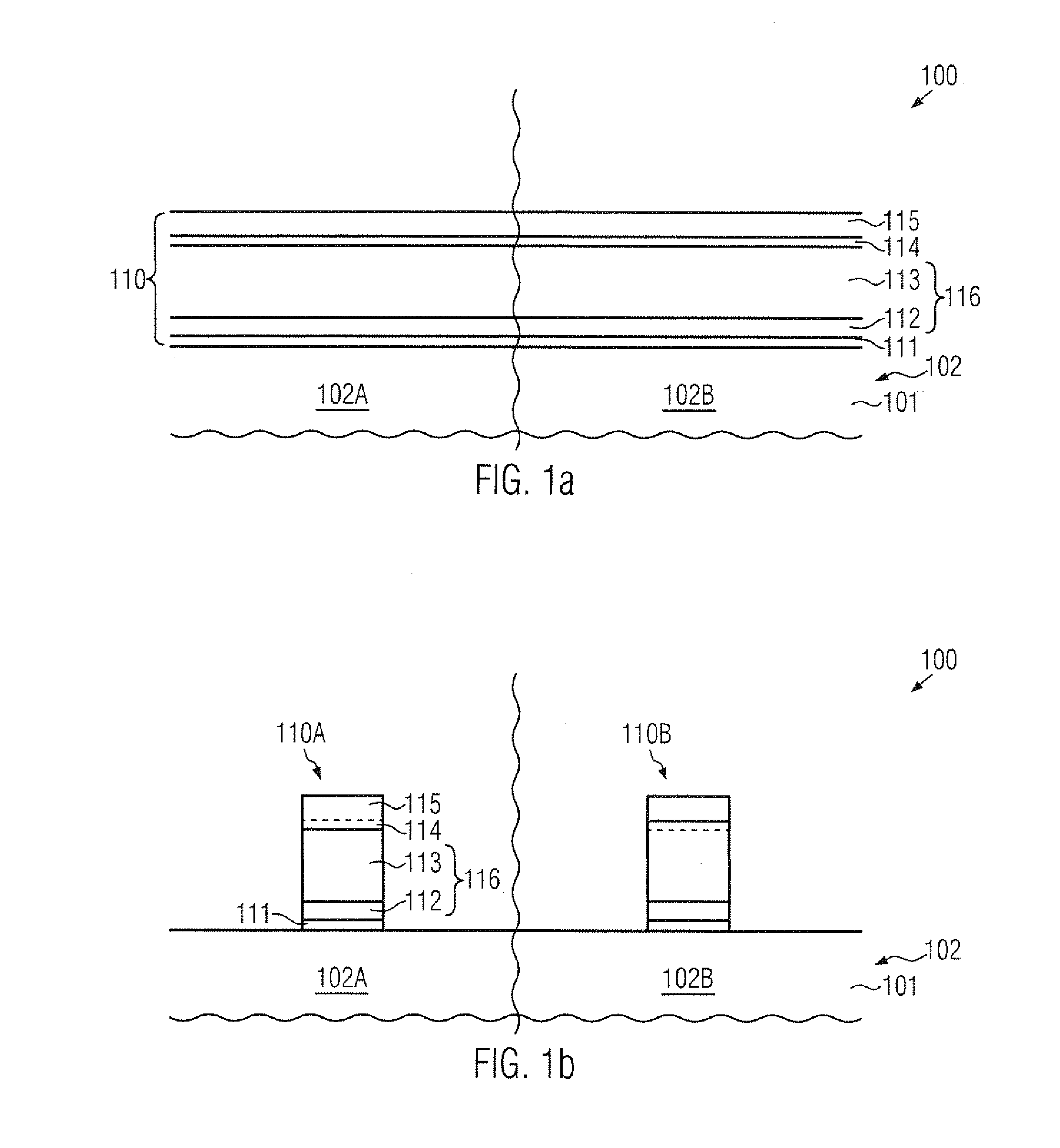
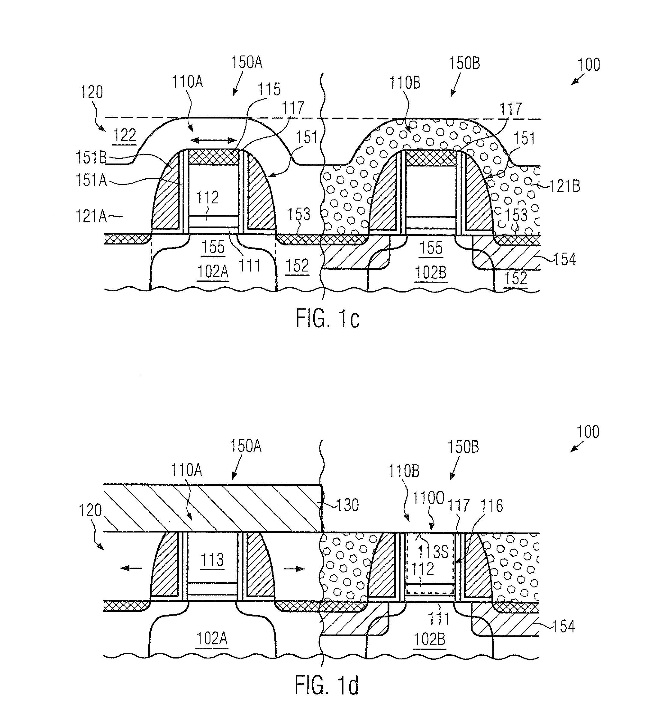
[0027]Various illustrative embodiments of the invention are described below. In the interest of clarity, not all features of an actual implementation are described in this specification. It will of course be appreciated that in the development of any such actual embodiment, numerous implementation-specific decisions must be made to achieve the developers' specific goals, such as compliance with system-related and business-related constraints, which will vary from one implementation to another. Moreover, it will be appreciated that such a development effort might be complex and time-consuming, but would nevertheless be a routine undertaking for those of ordinary skill in the art having the benefit of this disclosure.

[0028]The present subject matter will now be described with reference to the attached figures. Various structures, systems and devices are schematically depicted in the drawings for purposes of explanation only and so as to not obscure the present disclosure with details ...


PUM


Abstract

Sophisticated high-k metal gate electrode structures are provided on the basis of a hybrid process strategy in which the work function of certain gate electrode structures is adjusted in an early manufacturing stage, while, in other gate electrode structures, the initial gate stack is used as a dummy material and is replaced in a very advanced manufacturing stage. In this manner, superior overall process robustness in combination with enhanced device performance may be achieved.

Description

BACKGROUND OF THE INVENTION[0001]1. Field of the Invention[0002]Generally, the present disclosure relates to the fabrication of sophisticated integrated circuits including transistor elements comprising highly capacitive gate structures on the basis of a high-k dielectric material.[0003]2. Description of the Related Art[0004]The fabrication of advanced integrated circuits, such as CPUs, storage devices, ASICs (application specific integrated circuits) and the like, requires the formation of a large number of circuit elements on a given chip area according to a specified circuit layout, wherein field effect transistors represent one important type of circuit element that substantially determines performance of the integrated circuits. Generally, a plurality of process technologies are currently practiced, wherein, for many types of complex circuitry, including field effect transistors, CMOS technology is currently one of the most promising approaches due to the superior characteristi...

Claims


Application Information

Patent Timeline
30 Jun 2011
Publication
US20110156154A1
IPC
H01L27/092; H01L21/336
CPC
H01L21/28079; H01L29/7848; H01L21/31155; H01L21/823807; H01L21/823814; H01L21/823842; H01L29/165; H01L29/495
Inventors
HOENTSCHEL, JAN; BEYER, SVEN