[0006]The present invention provides alternative fabrications methods, that in part or as a whole can provide higher efficiency solar cells. It utilizes directed
implant techniques to form various emitter regions and doped
back surface field (BSF), both homogeneous and selective emitter regions in an interdigitated back surface contact (IBC)
cell, as well as formation of mesotaxial
layers (seed implants). The BSF can comprise homogeneous or selective emitter regions for interdigitated formation of alternative
doping regions in order to eliminate front surface shading. The present invention also addresses the formation of contacts to emitters and BSF regions through selective metallization, either by implantation,
laser, plating, or ink jet printing. The essence of the first discovery is the use of a very cost effective self-aligned selective
implant method that simplifies the
cell processing.
[0007]Some of the advantages of this methodology are to minimize the resistance of contact,
busbar, fingers,
contact resistance of
metal-
silicon interface, resistance of backside metallization, and achieving the desired resistivity under the grid contact and in between the fingers. Moreover, the advantageous formation of selective emitter and BSF and its ability to improve performance is made possible by the present invention. It can be applied to as-grown single or mono-crystalline, poly or multi-
crystalline silicon, as well as very thin film deposited
silicon, or other materials used for solar
cell formation and other applications. It can also be extended to
atomic species placement for any other material used in fabrication of junctions or contacts.
[0008]
Application specific ion implantation and annealing systems and methods are adopted to provide the appropriate placement of dopant both within the bulk of the material and laterally positioned across the substrate. Accordingly, the present invention can employ the fabrication methods and systems discussed in U.S.
patent application Ser. No. 12 / 483,017, entitled “FORMATION OF
SOLAR CELL-SELECTIVE EMITTER USING
IMPLANT AND ANNEAL METHOD,” filed Jun. 11, 2009, and in U.S. Provisional Application No. 61 / 131,698, entitled “FORMATION OF
SOLAR CELL-SELECTIVE EMITTER USING
IMPLANT AND ANNEAL METHOD,” filed Jun. 11, 2008, which are both hereby incorporated by reference as if set forth herein. These patent applications disclose the ability to independently control any species and dopant positioning and provide the necessary
surface concentration,
junction depth, and shape of the dopant profile. In these patent applications, an
Application Specific Implanter is described that can provide a plurality of dopants, selectively and otherwise. The present invention can also include the
impact of surface conditionings and variability of texturing discussed in U.S.
patent application Ser. No. 12 / 482,947, entitled “
APPLICATION SPECIFIC IMPLANT SYSTEM AND METHOD FOR USE IN SOLAR
CELL FABRICATIONS,” filed Jun. 11, 2009, and in U.S. Provisional Application No. 61 / 131,688, entitled “APPLICATIONS SPECIFIC IMPLANT
SYSTEM AND METHOD FOR USE IN SOLAR
CELL FABRICATIONS,” filed Jun. 11, 2008, which are both hereby incorporated by reference as if set forth herein. In present invention, the use of accurate and highly placed dopant and tailoring of dopant atomic profile methods are employed in order to provide heavily doped selective emitter regions (e.g., 10-40 Ohms / square) placed under the grid line, as well as methods to achieve lightly doped homogeneous emitter regions (e.g., 80-160 Ohms / square) in between grid fingers. Additionally, through the use of tailored parameters, the atomic dopant profile is simultaneously matched to provide the electrical junctions at the appropriate depth against the
substrate doping levels and provide the resistivity required for the formation of the contacts on the surface. In some embodiments, use of retrograde
doping and flat atomic profile (box junctions) are also employed. Furthermore, such capability will allow for independent doping of surfaces, such as emitter and BSF. Again, selective dopant capability can allow for an interdigitated
doping profile on the back surface that eliminates the front surface shadowing. It is proposed that such capability alone can provide efficiency gains in advance of 1 to 2 absolute percentage points.
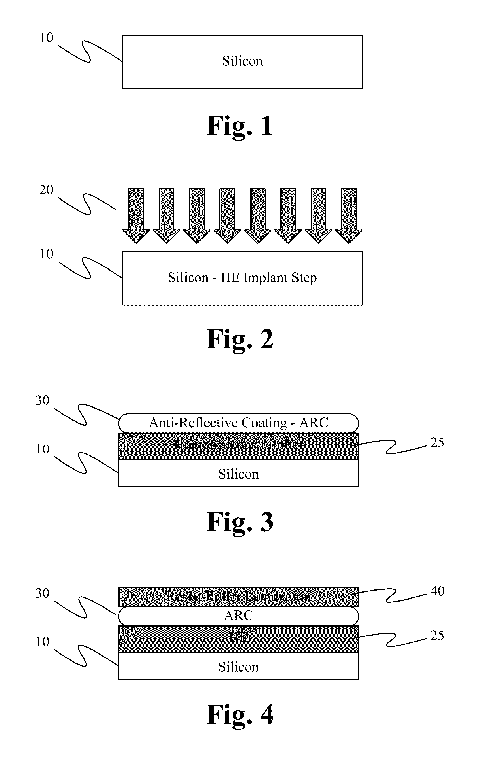
[0012]
Ion implantation can be used by the present invention to implant almost any species from the
periodic table into a semiconducting wafer. This capability can be used for the seeding implant, which is the subject of the previously referenced patent applications, whereby the appropriate element (metals or combination of different species) can be implanted at or near the surface of the semiconducting wafer, or in any film covering the surface, in order to provide an
initiation point for the subsequent growth or deposition of the same element (metal or otherwise) or other elements to form the necessary components of the solar cell (formation of contact, silicidation, etc.). This method can be used to affect the
work function of the
metal semiconductor interface or tailor the
band gap to enhance the performance of the solar cell, such as through improving the contacts. For this purpose, implantation of metals at medium to low levels can be used to seed and prepare the subsequent process. This implantation will minimize the need to adopt the use of high temperature firing methods employed today, resulting in a much lower temperature time regimes, and thereby avoiding the deleterious effects of multi-crystalline cells at high thermal budgets.
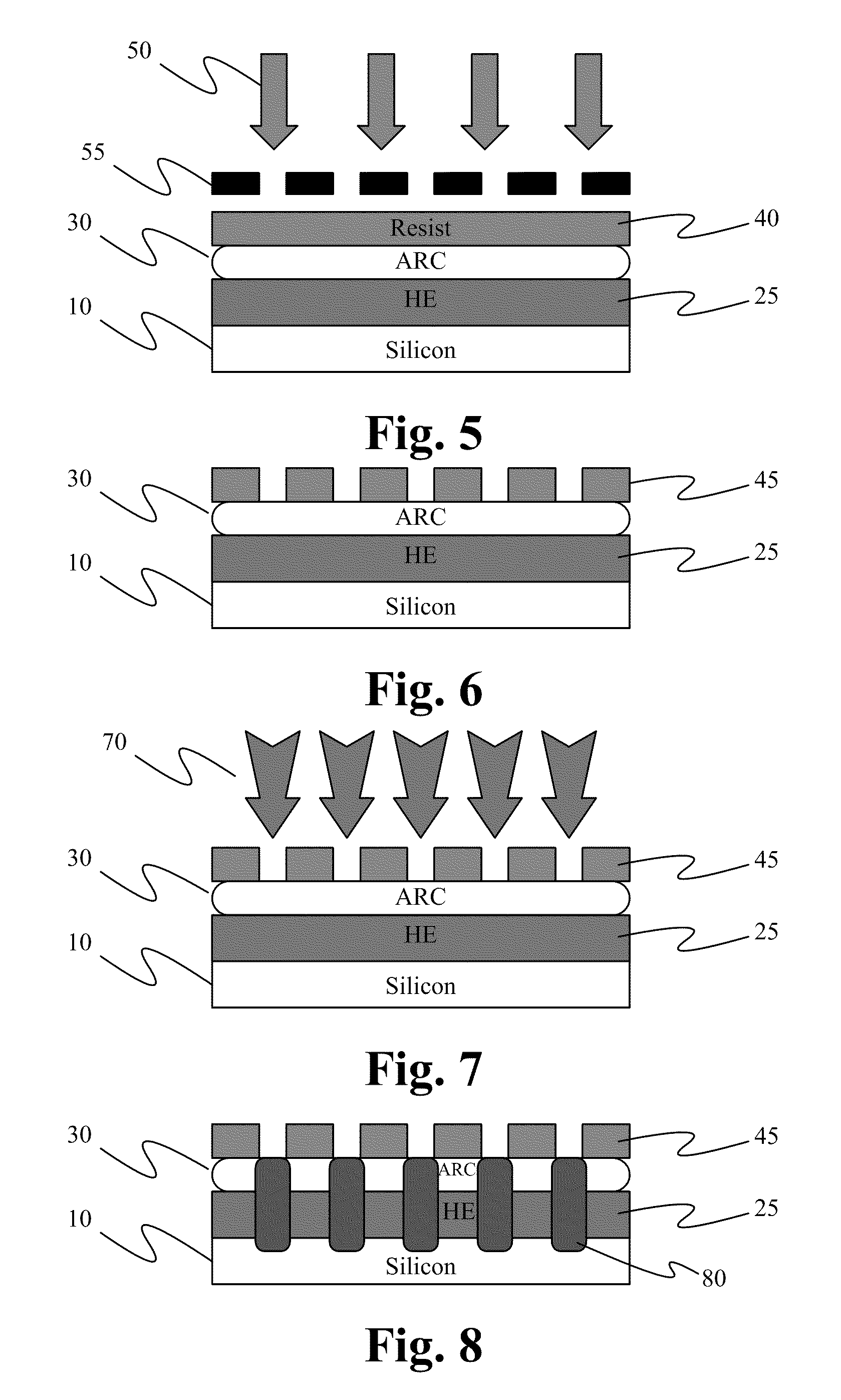
[0013]The selectivity of doping can be addressed in many different ways, as described in the previously referenced applications, where a
shadow mask is adopted to provide the selectivity required, as discussed in U.S. Provisional Application No. 61 / 302,861, entitled “AN ADJUSTABLE
SHADOW MASK ASSEMBLY FOR USE IN SOLAR
CELL FABRICATIONS,” filed Feb. 9, 2010, which is hereby incorporated by reference as if set forth herein. Another simple and cost
effective method is the use of in-contact
mask exposure and resists patterning prevalent in other industries. This method provides the exact selectivity required to dope the regions below the contact gridlines. The issue of subsequent alignment of the metal gridlines is a critical one and needs to be addressed with accuracies in sub-10's of microns. Such patterning eliminates the needs for such alignment. Furthermore, it provides a vehicle to adopt the inexpensive and cost efficient electro- and electro-less plating techniques, which is discussed below. Additionally, use of novel techniques, such as selective printing methods is also demonstrated here. It is expected that such fabrication methods will provide additional efficiency gains.
[0029]In some embodiments, the front surface of the semiconducting wafer is characterized by an absence of any metal contacts, thereby eliminating any front surface shadowing by metal contacts.

