Method and System for Manufacturing Silicon and Silicon Carbide

a manufacturing system and technology of silicon carbide, applied in the direction of crystal growth process, polycrystalline material growth, silicon compounds, etc., can solve the problems of high cost, difficult to put materials themselves into arc furnaces, and high electrical energy consumption, so as to achieve stable and continuous purification, reduce waste of energy and materials, and high purity and quality

Inactive Publication Date: 2011-10-06
TAKASHI TOMITA
View PDF9 Cites 4 Cited by
  • Summary
  • Abstract
  • Description
  • Claims
  • Application Information

AI Technical Summary

Benefits of technology

[0052]Silicon (55) can be stably and continuously purified by using silicon carbide (54) and silica (52) for material, applying energy by an electromagnetic field or a microwave and producing a condition shielded from the air. Silicon (55) generated by the method has extremely high purity and quality equivalent to a grade of a semiconductor can be secured.
[00

Problems solved by technology

As a result, much electrical energy was consumed.
As for the silica rock and the coke, high-purity those can be selected before usage and the cost is naturally increased, however, when th

Method used


Image

  • Method and System for Manufacturing Silicon and Silicon Carbide
  • Method and System for Manufacturing Silicon and Silicon Carbide
  • Method and System for Manufacturing Silicon and Silicon Carbide

Examples


first embodiment

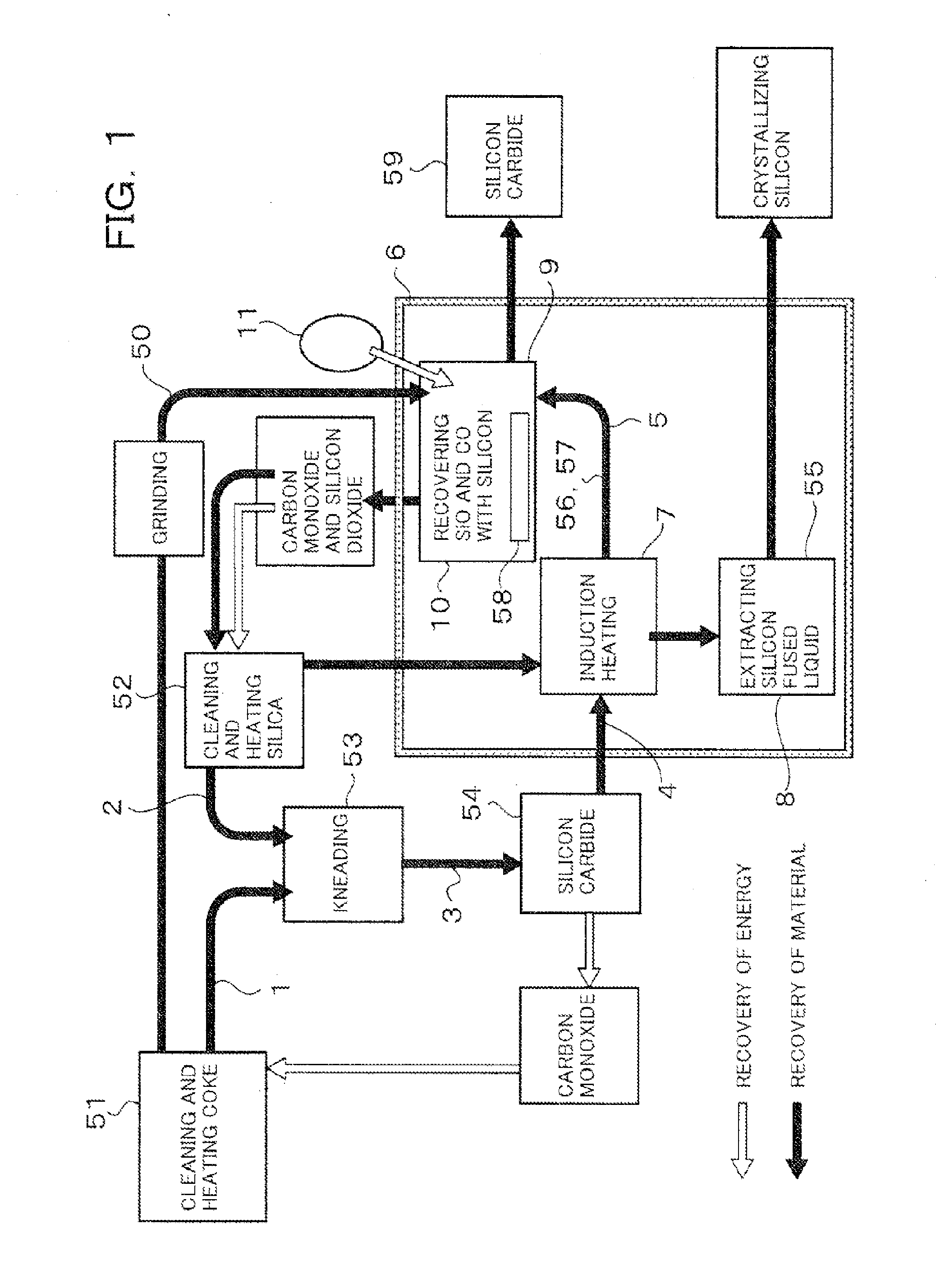
[0060]FIG. 1 is a schematic diagram for explaining the principle of a method of manufacturing silicon and silicon carbide according to the present invention. FIGS. 2A and 2B are schematic diagrams for illustrating an induction heating reactor used in the present invention.

[0061]Table 1 shows each content of boron, phosphorus, calcium, titanium, iron, nickel and copper which are respectively impurities in coke as material, cleaned coke, silica as material, cleaned silica, silicon carbide and silicon in units of ppm.

TABLE 1Table 1: Impurities Analysis.MaterialCleanedMaterialCleanedSiliconcokecokesilicasilicacarbideSiliconBoron80.250.1Phosphorus20110.1Calcium101301Titanium30.05400.1Iron200.5100.5Nickel100.550.5Copper100.5100.5

[0062]Coke as material (51) is ground in units of mm beforehand. Table 1 shows results of analyzing impurities in the carbon coke.

[0063]The coke as material is cleaned with aqueous solution. For a clearing solvent, HCN of 0.1 mol is used. After cleaning, the coke ...

second embodiment

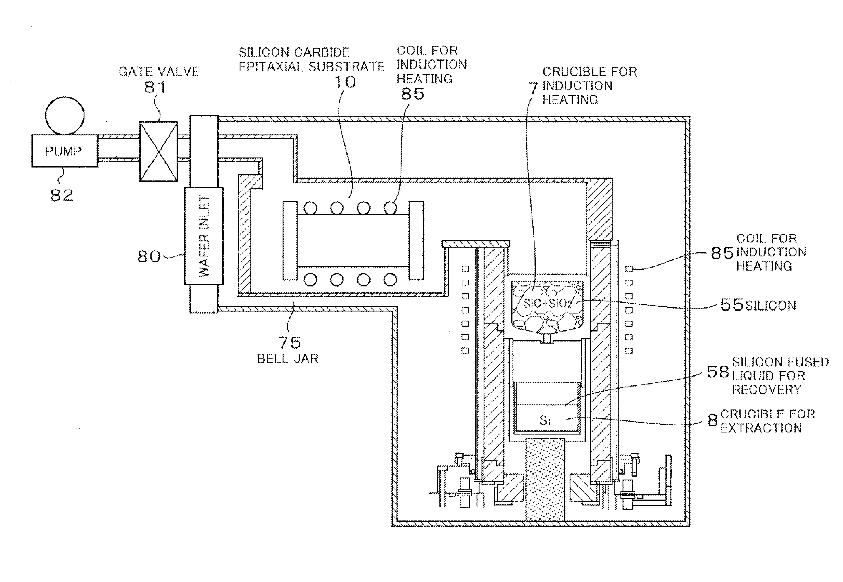
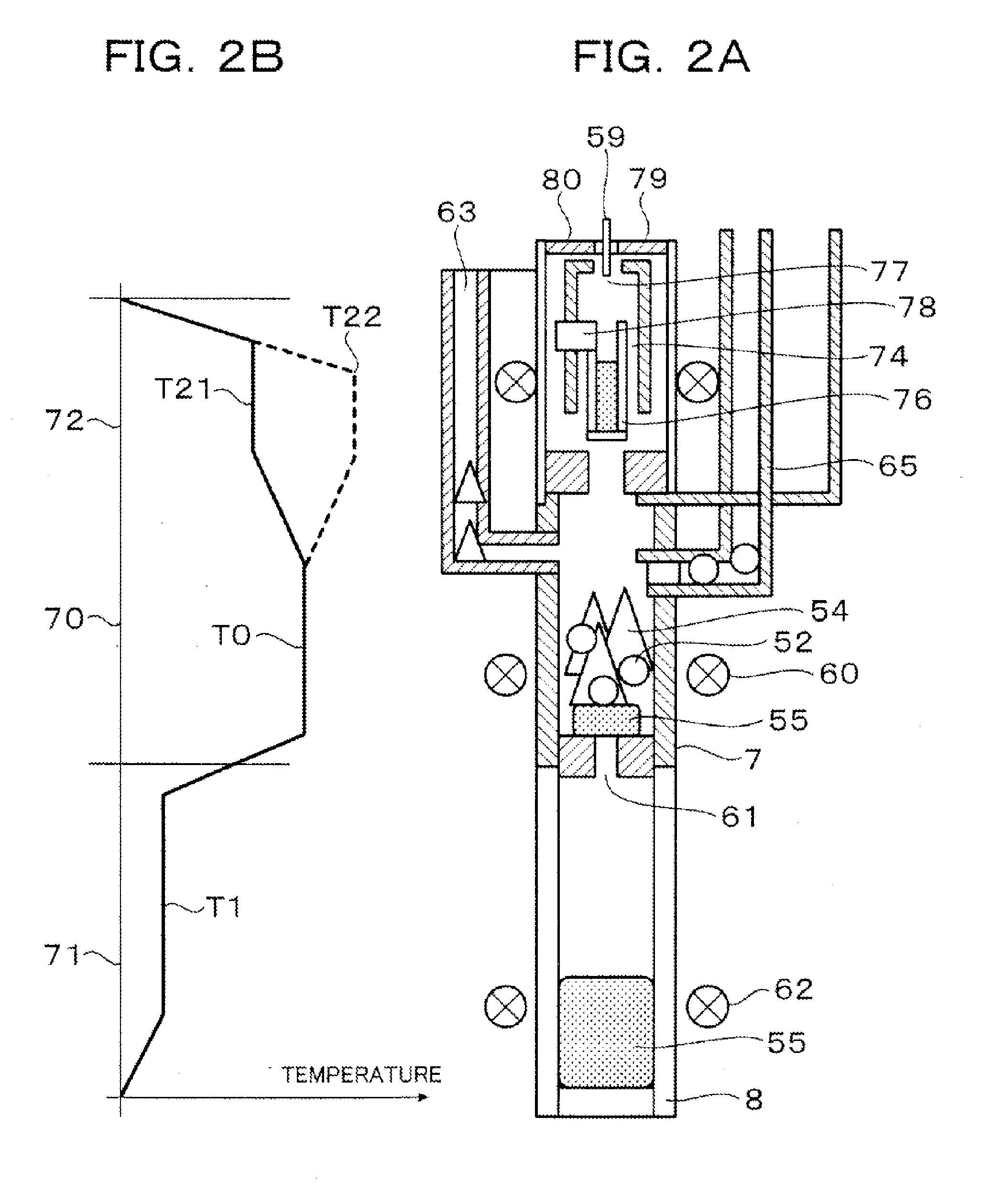
[0077]A second embodiment relates to configuration for integrating the above-mentioned reactional process so as to enhance efficiency in utilizing input energy. As shown in FIG. 2A, a basic process is the same as the basic process in the first embodiment and continuous production is aimed at. Heating is made using a coil (60) for induction heating according to a high-frequency induction method. Silicon carbide (54) is put into a crucible for heating (7) via a conduit tube (63). Silica (52) is put from the crucible for heating (7) through a conduit tube (65) into a silicon holding / solidifying crucible (8) through a silicon extracting hole (61). Hereby, silicon (55) is recovered.

[0078]The above-mentioned reactor is controlled to be temperature distribution at three stages. FIG. 2B shows the temperature distribution. An uppermost stage is equivalent to a reactor for growing silicon carbide (9) and the temperature (T2) is 1500 to 2500° C. A middle stage is equivalent to the crucible (7)...

third embodiment

[0084]In the above-mentioned embodiments, the multistage furnace in which the reactors are vertically arranged is used, however, as reactive gas is caused vigorously upward in the reactor at the uppermost stage, the surface of the wafer may be covered with silica when the wafer for recovering silicon carbide is put. To address this problem, a multistage furnace in which reactors are laterally arranged is provided. FIG. 4 shows the multistage furnace in the third embodiment. Carbon monoxide and silicon monoxide respectively caused from a crucible for heating (7) are laterally led. A surface of an input wafer can be prevented from being covered with silica by laterally arranging the reactor. Besides, as the reactor is laterally extended, more carbon monoxide and more silicon monoxide can be recovered.

[0085]For heating means, induction heating is used, however, it need scarcely be said that means such as electric resistance heating can be adopted.

[0086]In the present invention, high-pu...


PUM


Abstract

The present invention provides a method of manufacturing silicon and a manufacturing system for manufacturing and extracting silicon by grinding silicon carbide and silica, mixing each at predetermined ratio after cleaning them, housing them in a crucible, heating this by a heating unit to make them react, oxidizing the silicon carbide with the silica and further, reducing the silica with the silicon carbide. The present invention further provides a method of simultaneously manufacturing silicon and silicon carbide and a manufacturing system for producing silicon carbide by forming a silicon carbide film by vapor phase epitaxy using active gas generated in heating for reaction for material and recovering the silicon carbide film.

Description

BACKGROUND OF THE INVENTION[0001](1) Field of the Invention[0002]The present invention relates to a method and a system for manufacturing materials of silicon and silicon carbide used for a semiconductor, a solar cell and others.[0003](2) Description of the Related Art[0004]The present invention particularly relates to a method of reducing and manufacturing silicon for a high-purity semiconductor and a solar cell. For silicon manufacturing technology, heretofore, a method of generally using an arc furnace, individually putting carbon coke and silica rock (or silica sand) respectively as material into the furnace or mixing them and putting them into the furnace, supplying electrical energy from a carbon electrode installed with the carbon electrode hung from the upside, reducing silica and purifying silicon was used. This reactional process is mostly clarified and silicon generated by reaction in a dome including silica, carbon and fractional silicon carbide is extracted.[0005]Normal...

Claims


Application Information

Patent Timeline
IPC IPC(8): C01B31/36C01B33/025B01J19/00
CPCC01B33/025C30B29/36C30B25/02C01B32/984H01L21/20C01B32/97C01B33/023
Inventor TOMITA, TAKASHI
Owner TAKASHI TOMITA
Why Eureka
Try Eureka