Bonding film-attached substrate and bonding film-attached substrate manufacturing method

a film-attached substrate and film-attached technology, which is applied in the direction of instruments, record information storage, transportation and packaging, etc., can solve the problems of serious wavefront aberration, discoloration or adhesion failure, and difficulty in manufacturing methods

Inactive Publication Date: 2011-10-20
SEIKO EPSON CORP
View PDF6 Cites 24 Cited by
  • Summary
  • Abstract
  • Description
  • Claims
  • Application Information

AI Technical Summary

Benefits of technology

[0073]According to this application example configured as above, because the silicon oxide film is formed on the substrate by sputtering or vapor deposition in a temperature range of from 150° C. to 350° C., the silicon oxide film formed on the substrate is hard and dense, and can sufficiently prevent precipitation of foreign objects from the substrate surface. Further, because the bonding film is formed in a temperature range of from 40° C. to 150° C., the methyl group content falls in an optimum range, and the bonding film can be made flexible. Thus, the bonding film can sufficiently accommodate the bonding of the substrate and the adherend even when these substrates have different linear coefficients of expansion.

Problems solved by technology

However, the crystalline birefringent plate provided with a reflection preventing film or a UV-IR cut coating develops a warp in response to compressional stress or tensile stress, and as such the adhesive bonding of the crystalline birefringent plate to the IR absorbing glass or retardation plate produces nonuniform bonding layer thicknesses over the bonded surface, and causes serious wavefront aberrations.
Further, because the adhesive tends to undergo alteration by the reflow heat during the assembly of the optical low-pass filter, discoloration or adhesion failure occurs.
Further, the use of an adhesive often causes defects in a high-humidity environment, where the adhesive spreads out from the periphery of the bonded layer of the optical members in branch patterns.
However, the method involves difficulties in manufacture, because the direct bonding requires a high-temperature heat treatment (700 to 800° C.) of the substrate, or use of HF (hydrofluoric acid) during the hydrophilic treatment of the substrate bonding face.
The method also has a detachment problem, which occurs during the heat treatment or in a high temperature environment during manufacturing steps due to the different linear coefficients of expansion between the substrate materials and between substrate quartz crystal planes.
Another problem is that the bond strength becomes unstable depending on the conditions of the bonding face (such as uniformity, and cleanness).
However, Patent Documents 2, 3, and 4 do not disclose anything about a method of bonding an infrared cutoff filter element to a substrate such as a crystalline birefringent plate and a depolarizing plate (¼ wave plate).
However, these publications do not make detailed assessments concerning problems associated with different materials, or effectiveness of bonding for these materials.
Further, the glass substrate used for the infrared cutoff filter of Patent Document 1 is doped with CuO or other impurities for infrared absorption, and thus does not have chemical durability comparable to that of silicon oxide glass such as fused quartz.
Further, when the foreign objects precipitate in the bonded state, detachment becomes likely at the bond interface, and the bonding face pushes upward in different parts of the film and creates a space, which impairs the bonding film adhesion.
Further, because the bonding film bonding the quartz crystal and the translucent substrate cannot form siloxane (Si—O—Si) bonds with the translucent substrate, bonding reliability cannot be ensured.
The bond thus cannot withstand the heat strain that depends on temperature changes, and defects such as detachment at the bond interface occur, with the result that sufficient bond strength cannot be obtained.
That is, there is a problem that sufficient optical characteristics and reliability cannot be ensured for the optical element because of defects such as the detachment at the bond interface between the quartz crystal and the translucent substrate.
Specifically, it is difficult to obtain sufficient bond strength in bonding substrates of different materials, when the main component of the substrate is not silicon dioxide (SiO2), or when the substrate does not have a skeleton of Si groups.
However, because the titanium oxide itself does not have a sufficient amorphous structure, detachment may occur in the bonded film as a result of precipitation of foreign objects such as CuO.
The adhesion strength between the IR absorbing glass member and the titanium oxide film is therefore weak.
This impairs plane accuracy, and the bond strength becomes insufficient.
It is also difficult to control the number of methyl groups inside the bonding film.

Method used


Image

  • Bonding film-attached substrate and bonding film-attached substrate manufacturing method
  • Bonding film-attached substrate and bonding film-attached substrate manufacturing method
  • Bonding film-attached substrate and bonding film-attached substrate manufacturing method

Examples


second embodiment

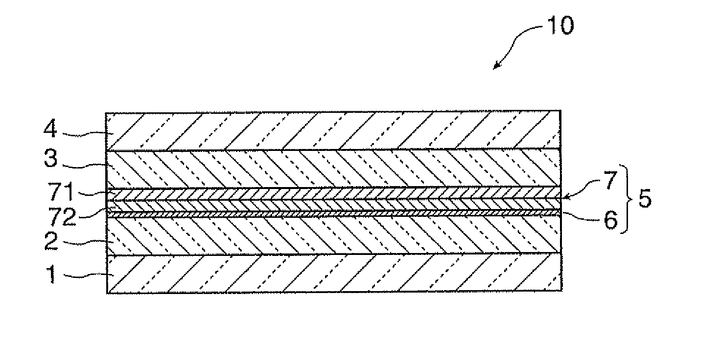
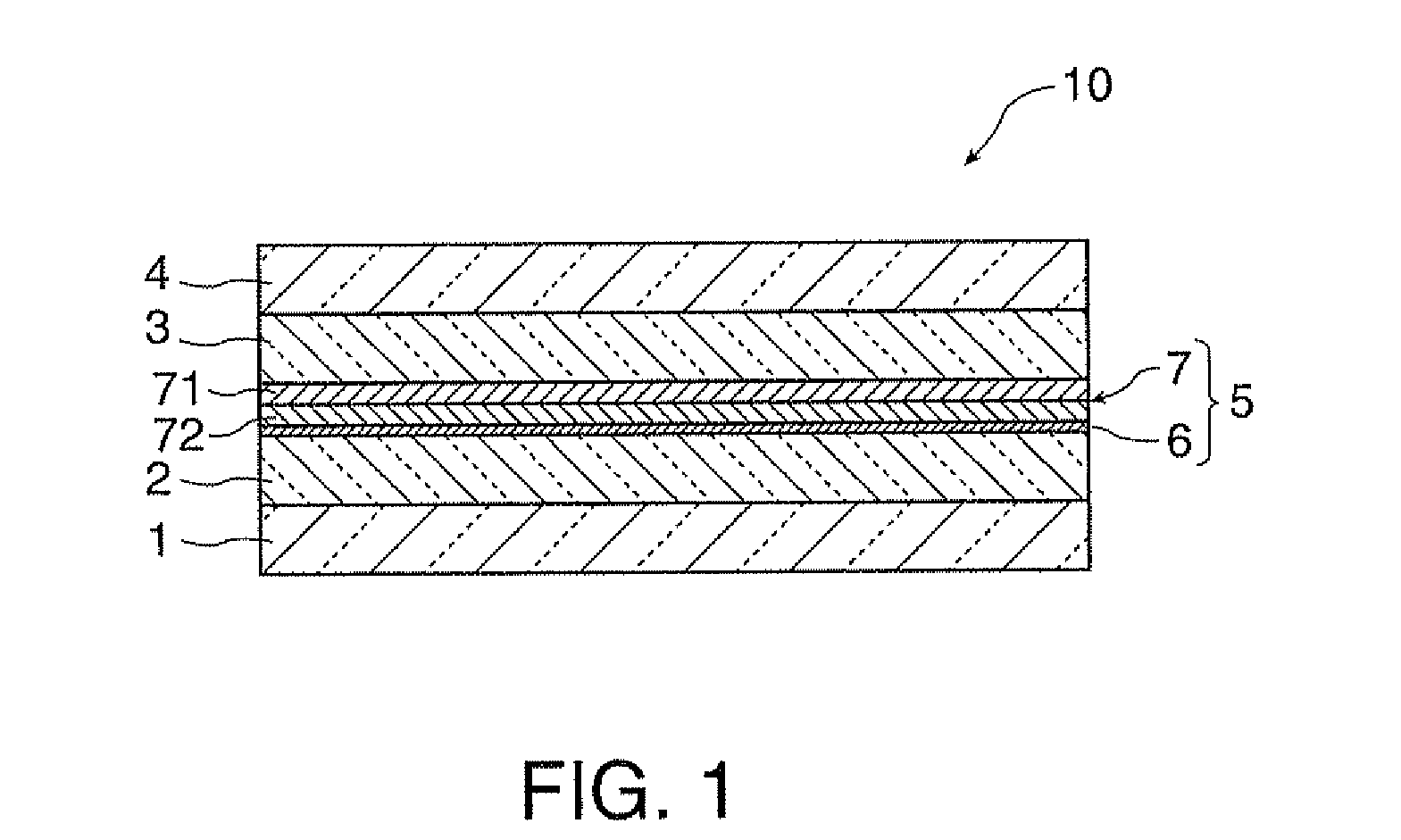
[0197]The following describes Second Embodiment of the present invention with reference to FIGS. 12A and 12B to FIGS. 16A and 16B. FIG. 12A is a schematic structure view illustrating an optical element provided with a bonding film-attached substrate according to Second Embodiment of the invention. FIG. 12B is a magnified cross sectional view illustrating a relevant portion of the optical element.

[0198]Second Embodiment is an example of the optical element as a polarization separation element 20, called a PS conversion element. The polarization separation element 20 is used by being incorporated in, for example, a liquid crystal projector.

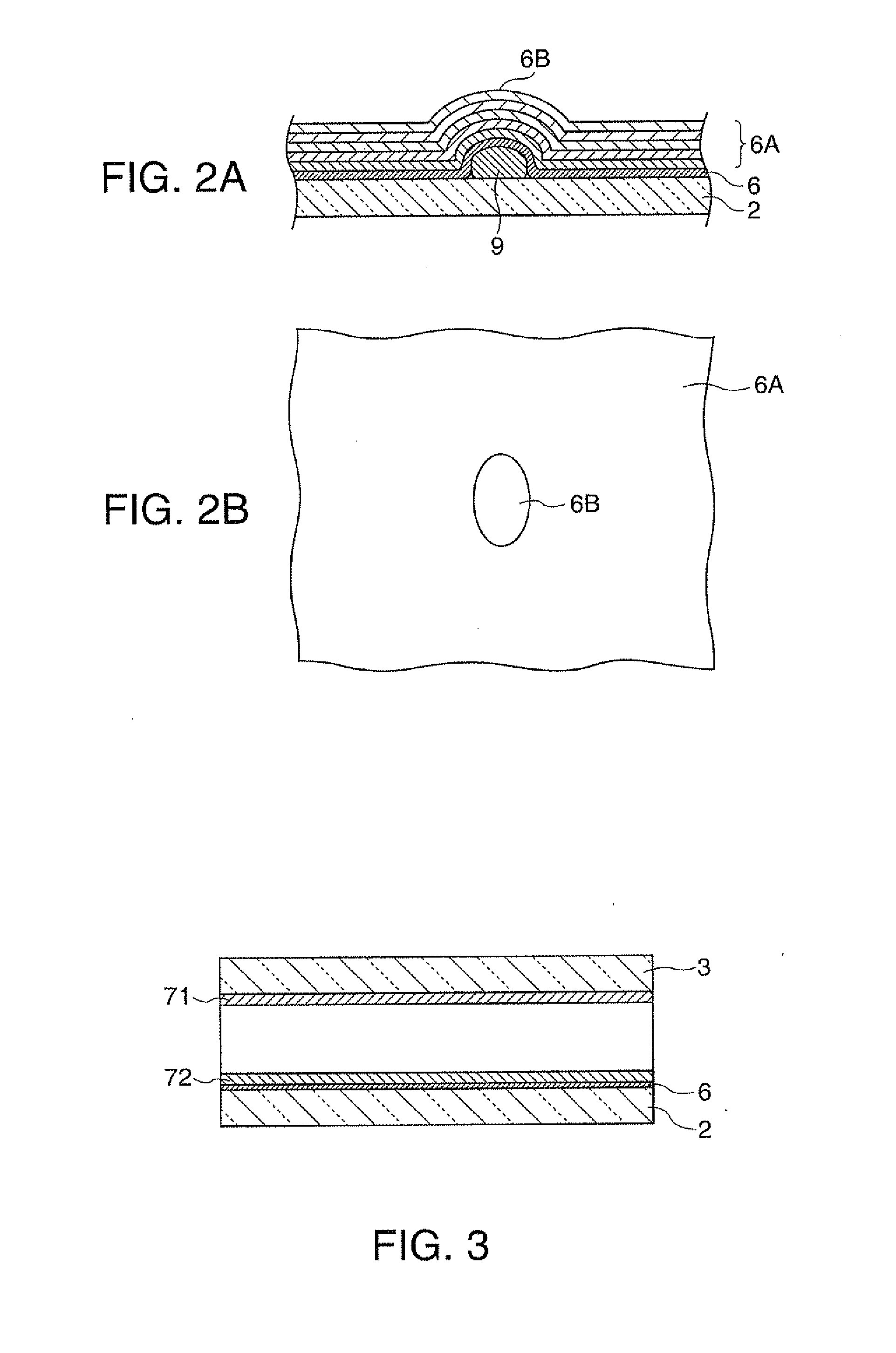
[0199]In FIGS. 12A and 12B, the polarization separation element 20 of Second Embodiment is shown as a laminate that includes a first glass-base material 23, and a second glass-base material 22 provided as a substrate bonded to the first glass-base material 23 via a polarization separation-conversion layer 21 or a reflecting film 24. Note that the se...

third embodiment

[0228]The following describes Third Embodiment of the present invention with reference to FIGS. 18A and 18B. FIG. 18A is a schematic plan view of an optical element provided with a bonding film-attached substrate according to Third Embodiment of the invention. FIG. 18B is a schematic structure view of the optical element.

[0229]Third Embodiment is an example of the optical element as an aperture filter 30. The aperture filter 30 is used by being incorporated in, for example, a pickup device.

[0230]As illustrated in FIGS. 18A and 18B, the aperture filter 30 of Third Embodiment includes a quartz crystal wave plate 31 (adherend), and a glass base material 32 provided as a substrate. Note that the glass base material 32 does not include silicon dioxide as the main component, or does not have a Si-group skeleton, and is, for example, a phosphate glass member.

[0231]The wave plate 31 includes a phase adjuster 311 and a wavelength selector 312. The phase adjuster 311 allows for passage of lig...

fourth embodiment

[0237]The following describes Fourth Embodiment of the present invention with reference to FIG. 19. FIG. 19 is a schematic plan view of an optical element provided with a bonding film-attached substrate according to Fourth Embodiment of the invention.

[0238]Fourth Embodiment is an example of the optical element as a diffraction grating-equipped wave plate 40 (hereinafter, simply “wave plate 40”). The wave plate 40 is used by being incorporated in, for example, a pickup device.

[0239]As illustrated in FIG. 19, the wave plate 40 of Fourth Embodiment is a laminate that includes a crystalline retardation plate 41 (adherend), a glass base material 42 provided as a substrate and bonded to a retardation plate 41, and a polarizing element 43 provided on the retardation plate 41 opposite from the glass base material 42. Note that the glass base material 42 does not include silicon dioxide as the main component, or does not have a Si-group skeleton, and is, for example, a phosphate glass member...


PUM

PropertyMeasurementUnit
thicknessaaaaaaaaaa
temperatureaaaaaaaaaa

Abstract

A bonding film-attached substrate includes: a substrate whose main component is not silicon dioxide, or that does not have a Si-group skeleton; a silicon oxide film formed on a surface of the substrate and adjacent to the substrate using a vapor-phase deposition method, and that has a thickness of from 100 nm to 2,000 nm, inclusive; and a bonding film provided by plasma polymerization, wherein the bonding film includes (i) a Si skeleton that contains a siloxane (Si—O) bond, and has a crystallinity of 45% or less, and (ii) an elimination group that binds to the Si skeleton, the elimination group being an organic group.

Description

BACKGROUND[0001]1. Technical Field[0002]The present invention relates to bonding film-attached substrates and bonding film-attached substrate manufacturing methods.[0003]2. Related Art[0004]Optical devices such as digital still cameras use optical low-pass filters (JP-A-2003-248198, Patent Document 1). In one variation, the optical low-pass filter is structured as a laminate of a crystalline birefringent plate, an IR (infrared) absorbing glass, a crystalline retardation plate (specifically, ¼ wave plate, also known as a depolarizing plate), and a crystalline birefringent plate. Of these optical components, the surface of the crystalline birefringent plate disposed on the outer side is coated with a reflection preventing film or a UV (ultraviolet)-IR cut coating.[0005]Known examples of IR absorbing glass include an infrared cutoff filter that includes an infrared absorbing film on a substrate that has an infrared absorbing function imparted by adding CuO to a phosphate glass base mat...

Claims


Application Information

Patent Timeline
Patent Type & Authority Applications(United States)
IPC IPC(8): B32B5/00C23C14/34B05D3/14G02B5/18
CPCB05D1/62C03C17/42C03C2218/15Y10T428/265C23C14/08G02B27/283G02B27/285C23C14/024
Inventor MATSUZAKI, FUMITAKEMIYABARA, MITSURUUEHARA, TAKEHIKO
Owner SEIKO EPSON CORP
Why Eureka
Try Eureka