Nanoscale High-Aspect-Ratio Metallic Structure and Method of Manufacturing Same

a high-aspect ratio, metallic structure technology, applied in the direction of paper/cardboard containers, containers, applications, etc., can solve the problems of high electricity consumption tariffs, high cost of solar cell panels, which have been continuously reducing for approximately 20 years, and achieve the effect of enhancing the performance of solar cells, leds and structures

Inactive Publication Date: 2012-02-09
IOWA STATE UNIV RES FOUND
View PDF6 Cites 25 Cited by
  • Summary
  • Abstract
  • Description
  • Claims
  • Application Information

AI Technical Summary

Benefits of technology

[0012]In view of the above, embodiments of the present invention provide a new and improved solar cell electrode and method of fabricating solar cell electrodes that overcome one or more of the problems existing in the art. More specifically, embodiments of the present invention provide new and improved method utilizing nano-scale high-aspect-ratio metallic structures that can be used to enhance the performance of solar c

Problems solved by technology

This translates into electric energy generation costs of approximately 20-25 cents/kW hour (kWh).
The daytime tariffs for electricity consumption in California are very high (approximately 15-20 cents/kWh), because the peak power produced during daytime relies on very expensive natural gas, which is now costing upward of $10.00/MMBTU.
Unfortunately, the costs of solar cell panels, after continuously reducing for approximately 20 years, have recently started to increase.
One reason is due to the cost of the silicon wafers, which typically use a very expensive feedstock made of purified polysilicon.
At these costs, electricity produced in sunny climates costs about 20-25 c/kWh, which is much too high to compete against power produced by conventional means, e.g., from coal.
Another factor contributing to the high cost of solar cells is the cost associated with the fabricating solar cell electrodes.
Currently, most solar cells, and even most solid-state lighting (SSL) devices,

Method used


Image

  • Nanoscale High-Aspect-Ratio Metallic Structure and Method of Manufacturing Same
  • Nanoscale High-Aspect-Ratio Metallic Structure and Method of Manufacturing Same
  • Nanoscale High-Aspect-Ratio Metallic Structure and Method of Manufacturing Same

Examples


Embodiment Construction

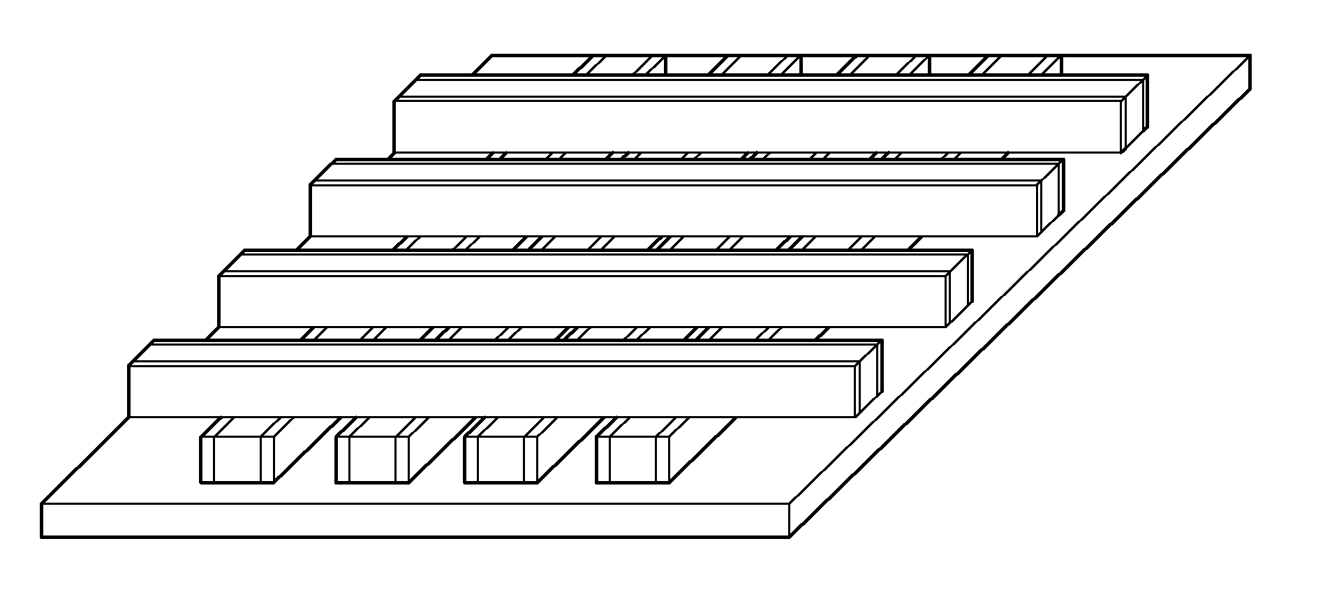
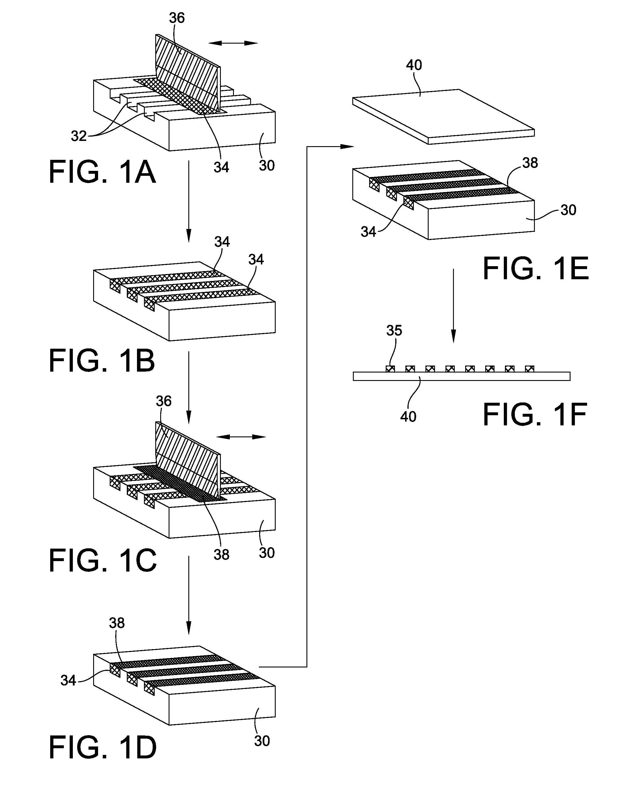
[0044]FIGS. 1A-1F are schematic diagrams that illustrate the steps of a two-polymer microtransfer molding (2-P μTM) process used in manufacturing an embodiment of the invention. Such a two-polymer microtransfer molding process is described in U.S. Pat. No. 7,625,515, entitled Fabrication of Layer-By-Layer Photonic Crystals Using Two Polymer Microtransfer Molding, to Lee et al., and assigned to the assignee of the instant application, the teachings and disclosure of which are hereby incorporated in their entireties herein by reference thereto. In at least one embodiment, the nanoscale metallic structures described herein are configured to provide plasmonic light concentration to enhance light absorption in solar cells, while also reflecting high amounts of infrared radiation.

[0045]As shown in FIGS. 1A-F, the photonic structure is prepared in a multiple stage process. PDMS (polydimethylsiloxane) or other suitable elastomeric molds 30 cast from a master pattern out of a photoresist rel...


PUM

PropertyMeasurementUnit
Angleaaaaaaaaaa
Angleaaaaaaaaaa
Angleaaaaaaaaaa

Abstract

Nanoscale high-aspect-ratio metallic structures and methods are presented. Such structures may form transparent electrode to enhance the performance of solar cells and light-emitting diodes. These structures can be used as infrared control filters because they reflect high amounts of infrared radiation. A grating structure of polymeric bars affixed to a transparent substrate is used. The sides of the bars are coated with metal forming nanowires. Electrodes may be configured to couple to a subset of the rails forming interdigitated electrodes. Encapsulation is used to improve transparency and transparency at high angles. The structure may be inverted to facilitate fabrication of a solar cell or other device on the back-side of the structure. Multiple layered electrodes having an active layer sandwiched between two conductive layers may be used. Layered electro-active layers may be used to form a smart window where the structure is encapsulated between glass to modify the incoming light.

Description

CROSS-REFERENCE TO RELATED PATENT APPLICATIONS[0001]This patent application is a Continuation-in-Part of co-pending U.S. patent application Ser. No. 13 / 026,637, filed Feb. 14, 2011, which claims the benefit of U.S. Provisional Patent Application No. 61 / 307,620, filed Feb. 24, 2010, the entire teachings and disclosure of which are incorporated herein by reference thereto.STATEMENT REGARDING FEDERALLY SPONSORED RESEARCH AND DEVELOPMENT[0002]This invention was made in part with Government support under Grant Numbers DE-ACO2-07CH11358 awarded by the Department of Energy. The Government has certain rights in this invention.FIELD OF THE INVENTION[0003]This invention generally relates to nanoscale high-aspect ratio metallic structures for use in solar cells and solid-state lighting devices, including organic light-emitting diodes.BACKGROUND OF THE INVENTION[0004]Since the turn of this century, awareness of climate change, the search for clean energy, and the need for utilizing energy effic...

Claims


Application Information

Patent Timeline
IPC IPC(8): H01L31/0232B05D5/06C23F1/04B32B37/02B32B37/14B05D3/00H01L31/18B05D5/12B82Y99/00
CPCB82Y30/00B82Y40/00Y10T156/10H01L51/442Y02E10/549H01L51/0023H10K71/621H10K30/82
Inventor KUANG, PINGPARK, JOONG-MOKLEUNG, WAIHO, KAI-MINGCONSTANT, KRISTEN P.CHAUDHARY, SUMIT
Owner IOWA STATE UNIV RES FOUND
Why Eureka
Try Eureka