Thermally enhanced semiconductor assembly with bump/base/flange heat spreader and build-up circuitry

a technology of heat spreader and semiconductor assembly, which is applied in the direction of circuit thermal arrangement, solid-state devices, basic electric elements, etc., can solve the problems of short life span, short life span, and immediate failure of semiconductor devices at high operating temperature, and achieve excellent heat spreading and heat dissipation, low cost, and low cost

Inactive Publication Date: 2012-05-24
BRIDGE SEMICON
View PDF0 Cites 24 Cited by
  • Summary
  • Abstract
  • Description
  • Claims
  • Application Information

AI Technical Summary

Benefits of technology

[0030]The present invention has numerous advantages. The heat spreader can provide excellent heat spreading and heat dissipation without heat flow through the adhesive. As a result, the adhesive and the substrate can be a low cost dielectric and not prone to delamination. The bump and the flange can be integral with one another, thereby providing excellent electromagnetic shielding and a moisture barrier for the semiconductor device, thereby enhancing electrical performance and environmental reliability. The mechanically-formed cavity in the bump can provide a well-defined space for semiconductor device placement. As a result, the semiconductor device shifting and cracking during lamination can be avoided, thereby enhancing manufacturing yield and reducing cost. The base can include a selected portion of the metal layer associated with the substrate, thereby enhancing thermal performance. The base can provide mechanical support for the substrate, thereby preventing warping. The adhesive can be sandwiched between the bump and the substrate, between the base and the substrate and between the flange and the substrate, thereby providing a robust mechanical bond between the heat spreader and the substrate. The build-up circuitry can provide electrical connections to the semiconductor device with plated metal without wire bonds or solder joints, thereby increasing reliability. The build-up circuitry can also provide signal routing with simple circuitry patterns or flexible multi-layer signal routing with complex circuitry patterns.

Problems solved by technology

The convergence of mobility, communication, and computing has created significant thermal, electrical and cost challenges to the semiconductor packaging industry.
For instance, semiconductor devices are susceptible to performance degradation as well as short life span and immediate failure at high operating temperatures.
Even though chip-level design is continuously reducing the operating bias voltage to get the benefit of reduced power, integrating more functions in a limited space often offsets this potential solution.
In addition, semiconductor devices are often susceptible to undesirable electromagnetic interference (EMI) or other inter-device interference when they are densely packed together.
The signal integrity of these devices can be adversely affected when they perform high frequency transmitting or receiving.
Since the plastic housing and the dielectric layer typically have low thermal conductivity, the PBGA provides poor heat dissipation.
However, since the wire-bonded I / O pads and lead frame type interposer have limited routing capability, the QFN package is not suitable for high performance, high input / output (I / O) devices.
However, as the routing circuitry of wafer level packaging is strictly constrained by the silicon area of the semiconductor chip, wafer level packaging is not suitable for most high pin count devices.
Although a supporting platform is created and thermal issues can be resolved, applying a pressure of about 370 kg / cm2 at a temperature of 100° C. to 200° C. to press the chip into the metal block is prohibitively cumbersome and prone to damage the chip.
Furthermore, since it is difficult to accurately position the chip in the metal substrate due to lateral displacement, and there is no bonding material to secure the embedded chip, voids and inconsistent bond lines arise between the chip and the heat slug.
As a result, the assembly suffers from high yield loss, poor reliability and excessive cost.
Since the plastic housing and the plastic materials typically have low thermal conductivity, this assembly provides poor heat dissipation.
Furthermore, as semiconductor chips are placed on a planar surface before lamination, misplacement during die attachment and lamination-induced chip cracking during the build-up process often result in high yield loss.
Since the molding material is typically a poor thermal conductor, the heat generated from the enclosed chip is blocked by the molding compound.
Even though a mechanical grinding fixture can grind off the backside of the encapsulating material in order to re-expose the chip and therefore lower thermal resistance, the slow grinding process of removing the hardened molding compound can be expensive for high volume manufacture.
Furthermore, since the interfacial surfaces between the chips and the encapsulating material would be exposed due to grinding off the backside encapsulating material, moisture penetration, voids and cracks at the interfaces can result in serious reliability concern.
However, plastic substrates such as epoxy or polyimide have low thermal conductivity which limit heat dissipation, whereas dielectrics with higher thermal conductivity such as epoxy filled with ceramic or silicon carbide have low adhesion and are prohibitively expensive for high volume manufacture.
Like other cavity type approaches, this approach suffers poor manufacturing throughput due to inconsistent cavity formation in the resin.
Furthermore, since the metal is deposited in the cavity by electroplating, it has limited thickness and does little to improve the package's thermal performance.
Since the cavity in the metal block is formed by etching or by micro-machining or by milling out a portion of the material, the major drawbacks include low yield and high cost.
Furthermore, inconsistent cavity depth control of the recess in the metal block results in low throughput and low yield in volume production.

Method used


Image

  • Thermally enhanced semiconductor assembly with bump/base/flange heat spreader and build-up circuitry
  • Thermally enhanced semiconductor assembly with bump/base/flange heat spreader and build-up circuitry
  • Thermally enhanced semiconductor assembly with bump/base/flange heat spreader and build-up circuitry

Examples


embodiment 1

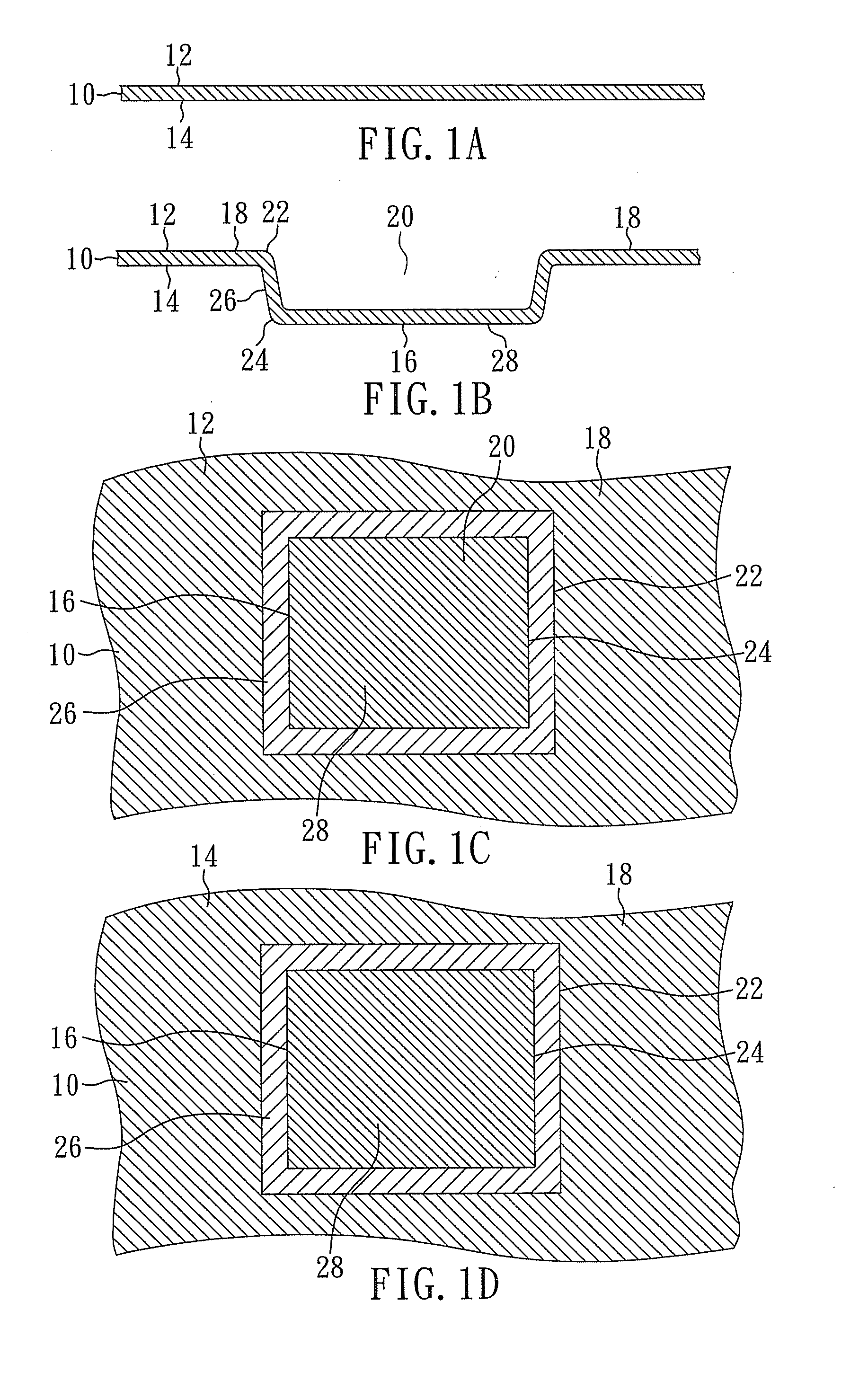
[0048]FIGS. 1A and 1B are cross-sectional views showing a method of making a bump and a flange in accordance with an embodiment of the present invention, and FIGS. 1C and 1D are top and bottom views, respectively, corresponding to FIG. 1B.

[0049]FIG. 1A. is a cross-sectional view of metal plate 10 which includes opposing major surfaces 12 and 14. Metal plate 10 is illustrated as a copper plate with a thickness of 100 microns. Copper has high thermal conductivity, good flexibility and low cost. Metal plate 10 can be various metals such as copper, aluminum, alloy 42, iron, nickel, silver, gold, combinations thereof, and alloys thereof.

[0050]FIGS. 1B, 1C and 1D are cross-sectional, top and bottom views, respectively, of metal plate 10 with bump 16, flange 18 and cavity 20. Bump 16 and cavity 20 are formed by mechanically stamping metal plate 10. Thus, bump 16 is a stamped portion of metal plate 10 and flange 18 is an unstamped portion of metal plate 10.

[0051]Bump 16 is adjacent to and i...

embodiment 2

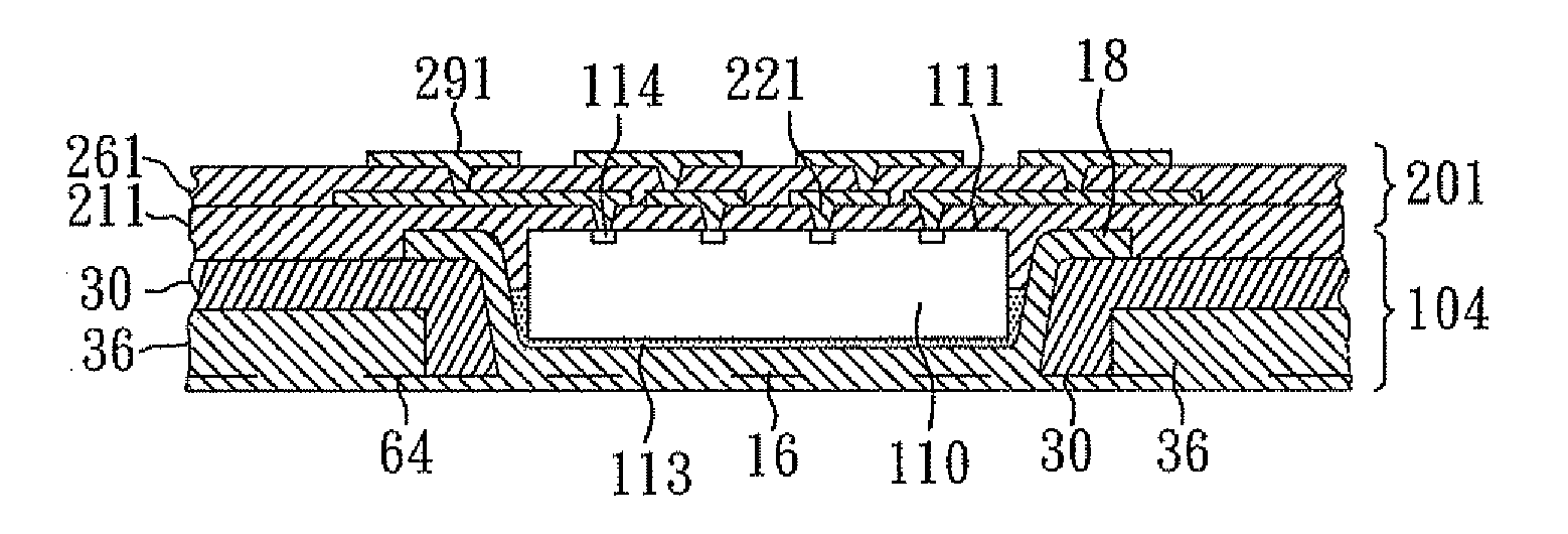
[0108]FIG. 6 is a cross-sectional view showing a semiconductor assembly that includes a thermal board with a substrate where first dielectric layer 211 is spaced from cavity 20 in accordance with another embodiment of the present invention.

[0109]In this embodiment, the semiconductor assembly is manufactured in a manner similar to that illustrated in Embodiment 1, except that die attach 113 fills the remaining space in cavity 20. As a result, die attach 113 fills the gap between bump 16 and semiconductor chip 110, and first dielectric layer 211 is deposited over the semiconductor chip top surface 111 (i.e. active surface), and contacts contact pads 114, die attach 113 and flange 18, but does not contact bump 16 and does not extend into cavity 20. For purposes of brevity, any description of thermal board 101 and build-up circuitry 201 is incorporated herein insofar as the same is applicable, and the same description need not be repeated. Likewise, elements of the thermal board and bui...

embodiment 3

[0110]FIG. 7 is a cross-sectional view showing a semiconductor assembly that includes a thermal board with a substrate where first conductive traces 241 are spaced from flange 18 in accordance with yet another embodiment of the present invention.

[0111]In this embodiment, the semiconductor assembly is manufactured in a manner similar to that illustrated in Embodiment 1, except that flange 18 is not exposed by first via openings 221, first conductive traces 241 do not extend to flange 18, and thus no electrical connection for flange 18 is provided. For purposes of brevity, any description of thermal board 101 and build-up circuitry 201 is incorporated herein insofar as the same is applicable, and the same description need not be repeated. Likewise, elements of the thermal board and build-up circuitry similar to those in thermal board 101 and build-up circuitry 201 have corresponding reference numerals.


PUM


Abstract

A semiconductor assembly includes a semiconductor device, a heat spreader, an adhesive and a build-up circuitry. The heat spreader includes a bump, a base and a flange. The bump defines a cavity. The semiconductor device is mounted on the bump at the cavity, electrically connected to the build-up circuitry and thermally connected to the bump. The bump extends from the base into an opening in the adhesive, the base extends vertically from the bump opposite the cavity and the flange extends laterally from the bump at the cavity entrance. The build-up circuitry includes a dielectric layer and conductive traces on the semiconductor device and the flange. The conductive traces provide signal routing for the semiconductor device.

Description

CROSS REFERENCE TO RELATED APPLICATION[0001]This application claims the benefit of filing date of U.S. Provisional Application Ser. No. 61 / 415,862, entitled “SEMICONDUCTOR CHIP ASSEMBLY WITH BUMP / BASE HEAT SPREADER, CAVITY IN BUMP AND EXTENDED CONDUCTIVE TRACE” filed Nov. 22, 2010 under 35 USC §119(e)(1).BACKGROUND OF THE INVENTION[0002]1. Field of the Invention[0003]The present invention relates to a semiconductor assembly, and more particularly to a thermally enhanced semiconductor assembly that includes a semiconductor device, a heat spreader, an adhesive and build-up circuitry.[0004]2. Description of Related Art[0005]The convergence of mobility, communication, and computing has created significant thermal, electrical and cost challenges to the semiconductor packaging industry. For instance, semiconductor devices are susceptible to performance degradation as well as short life span and immediate failure at high operating temperatures. Even though chip-level design is continuously...

Claims


Application Information

Patent Timeline
Patent Type & Authority Applications(United States)
IPC IPC(8): H01L23/498
CPCH01L21/56H01L23/3121H01L23/3677H01L23/49827H01L23/5389H01L23/552H01L24/19H01L24/20H01L24/24H01L24/82H01L25/105H01L2224/04105H01L2224/1132H01L2224/1146H01L2224/11849H01L2224/12105H01L2224/19H01L2224/2101H01L2224/211H01L2224/215H01L2224/221H01L2224/24101H01L2224/24221H01L2224/2929H01L2224/29339H01L2224/82106H01L2224/83192H01L2224/83862H01L2225/1035H01L2225/1041H01L2225/1058H01L2924/01012H01L2924/01013H01L2924/01029H01L2924/01079H01L2924/01082H01L2924/09701H01L2224/131H01L2924/01005H01L2924/01006H01L2924/01023H01L2924/01033H01L2924/0104H01L2924/01047H01L2924/01074H01L2924/01075H01L2924/01087H01L2924/014H01L2224/16225H01L2224/73267H01L2924/3511H01L2225/1023H01L2224/06181H05K1/0207H05K1/186H01L2924/0001H01L2224/92244H01L2224/0401H01L2924/1461H01L2224/13099H01L2924/00H01L2924/14H01L2924/15153H01L2924/181
Inventor LIN, CHARLES W. C.WANG, CHIA-CHUNG
Owner BRIDGE SEMICON
Why Eureka
Try Eureka