Device, thin film transistor, method for manufacturing the device and method for manufacturing the thin film transistor

a technology of thin film transistor and manufacturing method, which is applied in the direction of thermoelectric devices, photomechanical devices, instruments, etc., can solve the problems of inability to obtain a sufficient thickness of film, and achieve the effects of preventing damage to a member, preventing degradation of functional thin film or deteriorating life characteristics, and low energy

Inactive Publication Date: 2012-12-20
PANASONIC CORP +1
View PDF0 Cites 15 Cited by
  • Summary
  • Abstract
  • Description
  • Claims
  • Application Information

AI Technical Summary

Benefits of technology

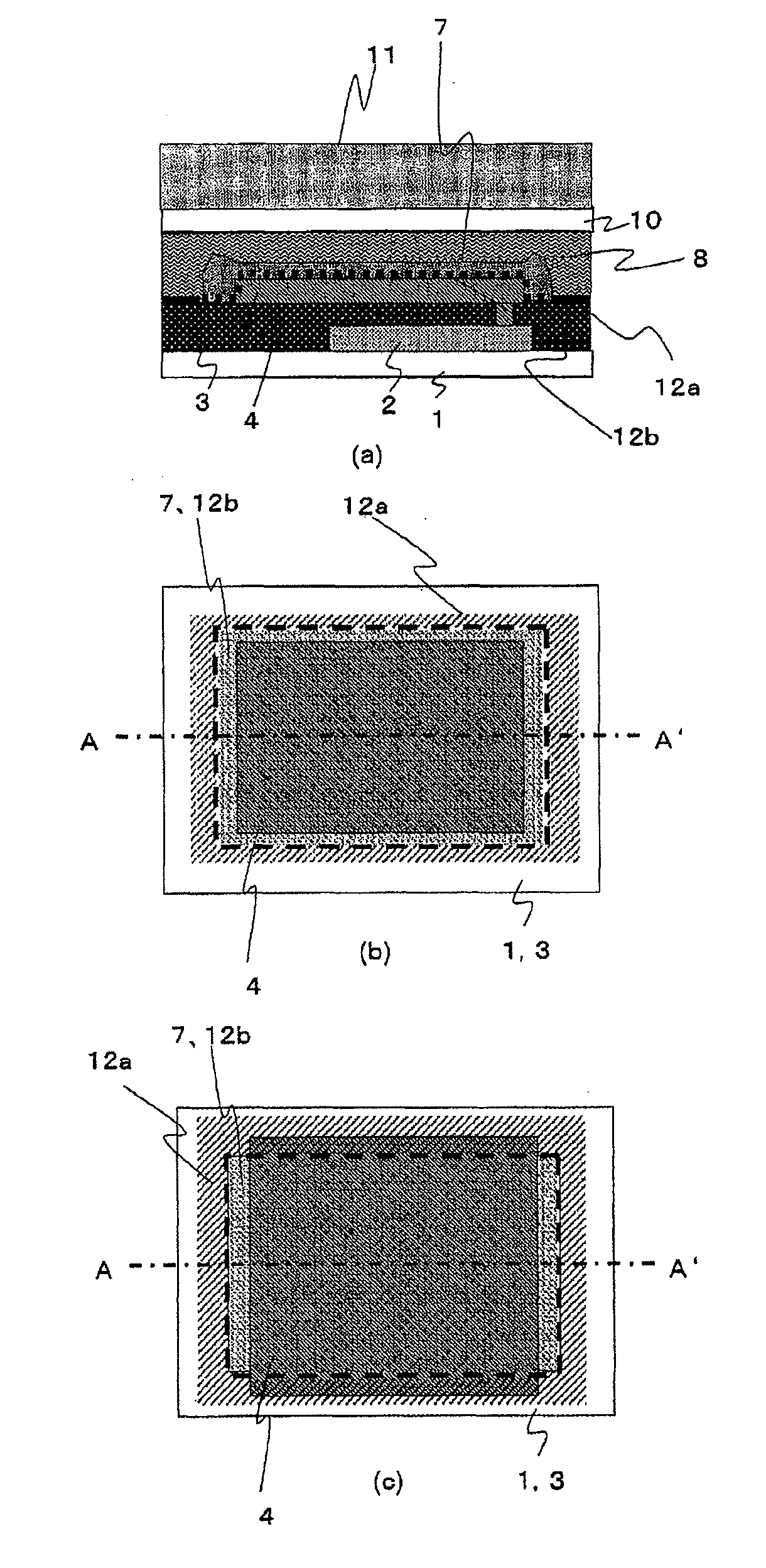
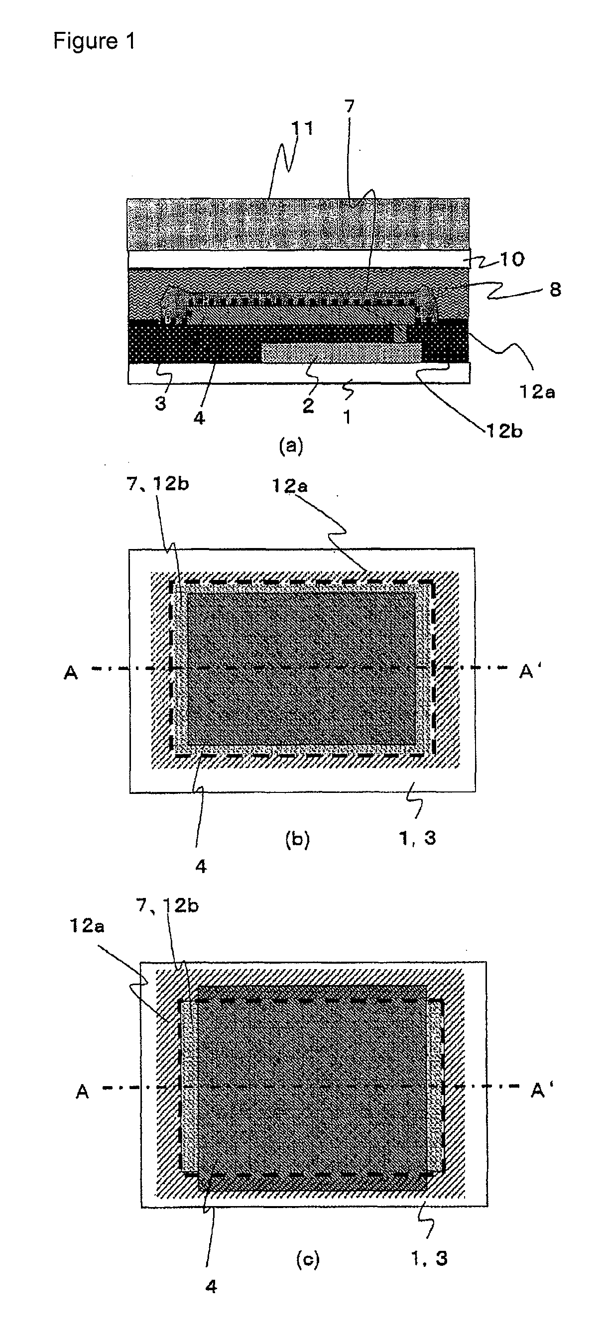
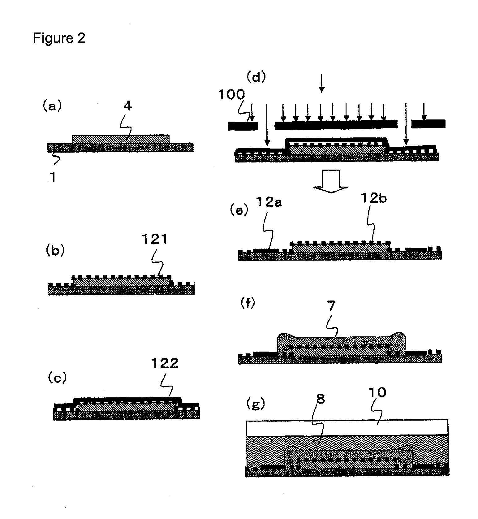
[0023]In accordance with an embodiment of the present invention, since processing for imparting liquid-repellency can be performed with light with relatively low energy without applying a photopolymerization initiator or a photocatalyst, it is possible to prevent damages to a member composing a substrate or a substrate surface to which the functional thin film is applied and prevent the molecules in the damaged member from diffusing in the functional thin film. As a result of this, degradation of characteristics of the functional thin film or deterioration of life characteristics can be prevented and a device adequately exhibiting functions of the functional thin film can be constructed.

Problems solved by technology

However, in this method, there is a problem that the applied ink rises and spreads along the bank, and therefore a film having a sufficient thickness cannot be obtained.

Method used


Image

  • Device, thin film transistor, method for manufacturing the device and method for manufacturing the thin film transistor
  • Device, thin film transistor, method for manufacturing the device and method for manufacturing the thin film transistor
  • Device, thin film transistor, method for manufacturing the device and method for manufacturing the thin film transistor

Examples


synthesis example 1

Synthesis of Compound 1

[0172]

[0173]Into a 200 ml two-necked eggplant flask, 1.0 g (4.5 mmol) of 9-anthracenecarboxilic acid, 0.93 g (4.5 mmol) of DCC (N,N′-dicyclohexylcarbodiimide) and 0.61 g (4.5 mmol) of HOBt (1-hydroxybenzotriazole) were put, and the flask was deaerated and the atmosphere in the flask was replaced with argon. To this, 360 ml of dry CH2Cl2 (dehydrated methylene chloride), 1.0 g (4.5 mmol) of APS (3-aminopropyltrimethoxysilane) and 0.45 g (4.5 mmol) of Et3N (triethylamine) were added, and the resulting mixture was magnetically stirred at room temperature for 24 hours. Since the progress of a reaction was confirmed by use of TLC (developing solvent: chloroform), the reaction was terminated, and after the solvent was distilled off under a reduced pressure, the product was purified by column chromatography (silica gel, developing solvent: chloroform). The yield was 360 mg (0.85 mmol, percent yield 20%).

[0174]1H NMR (CDCl3): δ=8.46 (s, 1H), 8.07 (d, 2H), 7.99 (d, 2H),...

synthesis example 2

Synthesis of Compound 2-1

[0175]

[0176]Into a three-necked round-bottom flask equipped with a Dimroth condenser and a septum cover, 268 mg (1.5 mmol, 1.0 eq.) of methyl gallate, 3.0 g (0.51 mmol, 3.5 eq.) of heptadecafluoroundecyliodo, 115 mg (0.043 mmol, 0.3 eq.) of 18-crown 6-ether, and 760 mg of potassium carbonate were put, and the flask was deaerated and the atmosphere in the flask was replaced with argon. 20 ml of dehydrated acetone was added and the resulting mixture was refluxed for 3 days. After confirming that the raw material was dissipated by use of TLC (developing solvent: hexane / ethyl acetate=5 / 1), the reactant was washed with distilled water and dried over anhydrous sodium sulfate, and then the solvent was distilled off under a reduced pressure. Purification of the product was carried out through recrystallization (acetone). The yield of a compound 2-1 was 2.0 g (1.3 mmol, percent yield 89%).

[0177]1H NMR (CDCl3): δ=7.28 (s, 2H), 4.11 (t, 3H), 4.05 (t, 2H), 3.89 (s, 3H),...

synthesis example 3

Synthesis of Compound 2-2

[0178]

[0179]Into a 100 ml three-necked round-bottom flask equipped with a Dimroth condenser and a septum cover, 49.5 mg (1.9 mmol, 2.0 eq.) of lithium aluminum hydride was put, and the flask was deaerated and the atmosphere in the flask was replaced with argon. To this, 10 ml of dehydrated THF (tetrahydrofuran) and 1.5 g (1.0 mmol) of the compound 2-1 were added and the resulting mixture was refluxed for 2 hours. After confirming that the raw material was dissipated by use of TLC (developing solvent: hexane / ethyl acetate=1 / 1), the solvent was distilled off under a reduced pressure. Purification of the product was carried out through recrystallization (acetone). The yield of a compound 2-2 was 1.4 g (0.91 mmol, percent yield 91%).

[0180]1H NMR (CDCl3): δ=6.59 (s, 2H), 4.60 (d, 2H), 4.06 (t, 4H), 3.97 (t, 2H), 2.33 (m, 6H), 2.15 (m, 4H), 2.08 (m, 2H)


PUM

PropertyMeasurementUnit
wavelengthaaaaaaaaaa

Abstract

A problem of the present invention is to provide a device having good characteristics and long life, wherein a functional thin film is formed in a desired region by a coating method; a thin film transistor; a method for producing the device; and a method for producing the thin film transistor. This problem can be solved by a device comprising: a substrate, a first electrode formed on the substrate, a functional thin film formed above the first electrode, and a second electrode disposed above the functional thin film, characterized by further comprising, in a region surrounding the region where the functional thin film is formed, a film containing a compound in which a group containing fluorine and a π-conjugated system are bound together by a cycloalkene structure or a cycloalkane structure.

Description

TECHNICAL FIELD[0001]The present invention relates to a device having a functional thin film, a thin film transistor, a method for producing the device and a method for producing the thin film transistor.BACKGROUND ART[0002]In the field of an organic thin film transistor device, an organic thin film solar cell, an organic EL display and the like, many functional thin films are investigated. The functional thin film is a thin film subjected to so-called fine patterning, which includes a material exhibiting various functions and is arranged at locations where the functions needs to be exhibited in a device with precision required for exhibiting the functions. Examples of the functions to be exhibited by patterning include functions of wiring, an electrode, an insulating layer, a light-emitting layer, a charge transporting layer and the like. As a technique of performing such patterning, an ink-jet method, a nozzle coating method, and various roll printing methods, for example, a metho...

Claims


Application Information

Patent Timeline
Patent Type & Authority Applications(United States)
IPC IPC(8): H01L51/30H01L51/46H01L51/40H01L51/54
CPCC09K11/06C09K2211/1007C09K2211/1011C09K2211/1029H01L27/3246G03F7/0046H01L51/0558H01L51/56H01L2227/323H05B33/10H01L51/0512H10K59/122H10K10/462H10K10/484H10K59/1201H10K71/00
Inventor SHINKAI, SEIJIHARAGUCHI, SHUICHISHIRAKE, TOMOHIROOGAWA, MASASHINAKATANI, SHUHEISAKANOUE, KEIGOTO, OSAMUKAKIMOTO, HIDENOBU
Owner PANASONIC CORP
Why Eureka
Try Eureka