
Unitary graphene layer or graphene single crystal

a graphene monolith and graphene technology, applied in the field of graphitic materials, can solve the problems of low strength of flexible graphite foils, poor structural integrity, and inability to produce this type of large unitary graphene entity from existing natural or synthetic graphite particles, and achieve high structural integrity, exceptional thermal conductivity, and low density

Active Publication Date: 2014-05-29
GLOBAL GRAPHENE GRP INC
View PDF4 Cites 58 Cited by
  • Summary
  • Abstract
  • Description
  • Claims
  • Application Information

AI Technical Summary

Benefits of technology

This patent describes a new material, called graphene oxide gel-derived unitary or monolithic graphene layer or graphene single crystal. This material has outstanding properties, including high thermal conductivity, electrical conductivity, mechanical strength, scratch resistance, and does not have any surface graphite flakes or particles that could peel off. The material has a unique combination of these properties and can be used as a heat spreader or heat sink for various applications, such as handheld devices, microelectronic or telecommunication devices, LED lighting devices, and so on. The material is lightweight, strong, and has superior surface hardness and scratch resistance compared to metal and ceramic materials. It also has low tendency to emit graphite or carbon particles into the air.

Problems solved by technology

It has not been possible to produce this type of large unitary graphene entity from existing natural or synthetic graphite particles.
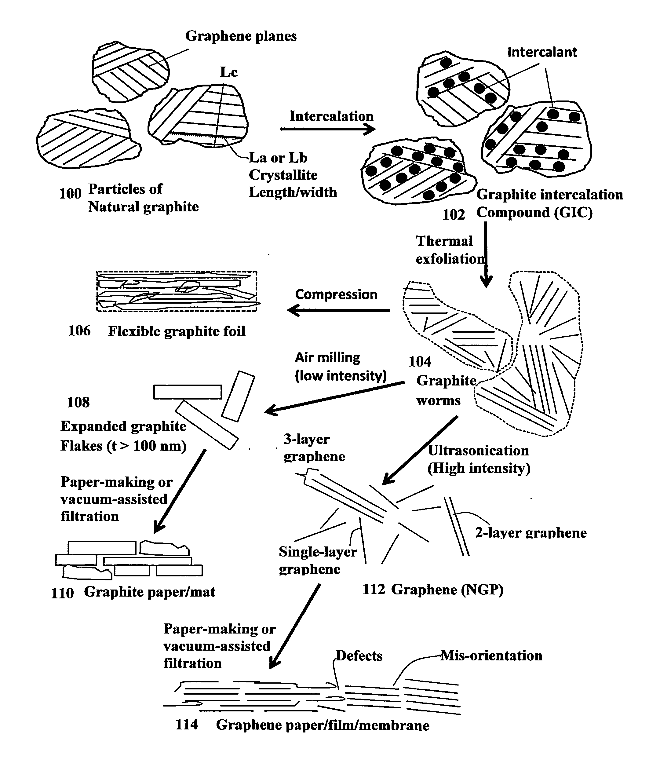
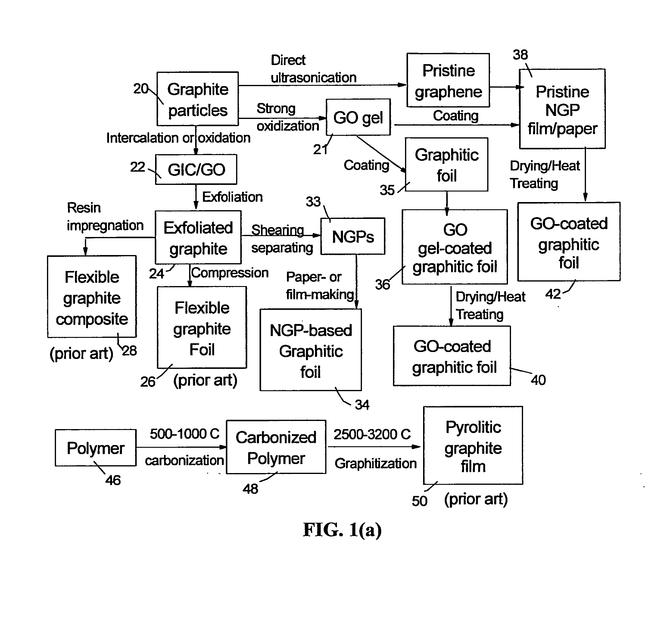
It may be noted that flexible graphite foils (obtained by re-compressing exfoliated graphite worms) for electronic device thermal management applications (e.g. as a heat spreader) have the following major deficiencies:(1) As indicated earlier, flexible graphite (FG) foils exhibit a relatively low thermal conductivity, typically (2) Flexible graphite foils are also of low strength and poor structural integrity.
The high tendency for flexible graphite foils to get torn apart makes them difficult to handle in the process of integrating them in a microelectronic device.(3) Another very subtle, largely ignored or overlooked, but critically important feature of FG foils is their high tendency to get flaky with graphite flakes easily coming off from FG sheet surfaces and emitting out to other parts of a microelectronic device.
This resin coating is typically not a thermally or electrically conductive material that is often an undesirable feature in a situation where high conductivity is required.
In other situations where electrical insulation or isolation is required, this resin layer can present some issues (e.g. mis-match in coefficients of thermal expansion and elastic constants between the FG layer and the resin coating, resulting in delamination or peeling-off after some number of thermal cycles).
For instance, although individual CNTs or CNFs alone can exhibit a high thermal conductivity (1,500-3000 W / mK), the resulting CNT or CNF paper or mat typically exhibit an in-plane thermal conductivity less than 100 W / mK and often less than 10 W / mK, likely due to the few and poor contacts between individual CNT or CNF filaments, providing insufficient cross-sections for electron flow or even impeding electron flow.
Further, the contact between a sheet-like graphitic layer and a heat source is usually poor due to limited contact surfaces between such a graphitic layer (e.g. CNT paper) and a rigid device component (e.g. a CPU in a mobile phone).
This results in an ineffective heat transfer between the heat source and the graphitic layer.
However, ultra-thin film or paper sheets (<10 μm) are difficult to produce in mass quantities, and difficult to handle when one tries to incorporate these thin films as a heat spreader material during the manufacturing of microelectronic devices.
Further, thickness dependence of thermal conductivity (not being able to achieve a high thermal conductivity at a wide range of film thicknesses) is not a desirable feature.
In general, paper made from platelets of graphene, graphene oxide, and RGO (e.g. those paper sheets prepared by vacuum-assisted filtration process) exhibit many defects, wrinkled or folded graphene sheets, interruptions or gaps between platelets, and non-parallel platelets (e.g. SEM image in FIG. 3(b)), leading to poor thermal conductivity and electric conductivity.
These papers or aggregates of discrete NGP, GO or RGO platelets also have a tendency to get flaky, emitting conductive particles into air.
Again, these aggregates have a great tendency to have graphite particles flaking and separated from the film surface, creating internal shorting problem for the electronic device containing these aggregates.
They also exhibit low thermal conductivity unless made into thin films (10 nm-300 nm, as reported by Haddon, et al) which are very difficult to handle in a real device manufacturing environment.
However, metal matrix material is too heavy and the resulting metal matrix composite does not exhibit a high thermal conductivity.
This is a slow, tedious, and energy-intensive process.
Furthermore, carbonization of certain polymers (e.g. polyacrylonitrile) involves the emission of toxic species.
This entails a thermo-mechanical treatment of combined mechanical compression and ultra-high temperature for an extended period of time in a protective atmosphere; a very expensive, energy-intensive, and technically challenging process.
The process requires high vacuum and ultra-high temperature equipment that is not only very expensive to make but also very expensive and difficult to maintain.
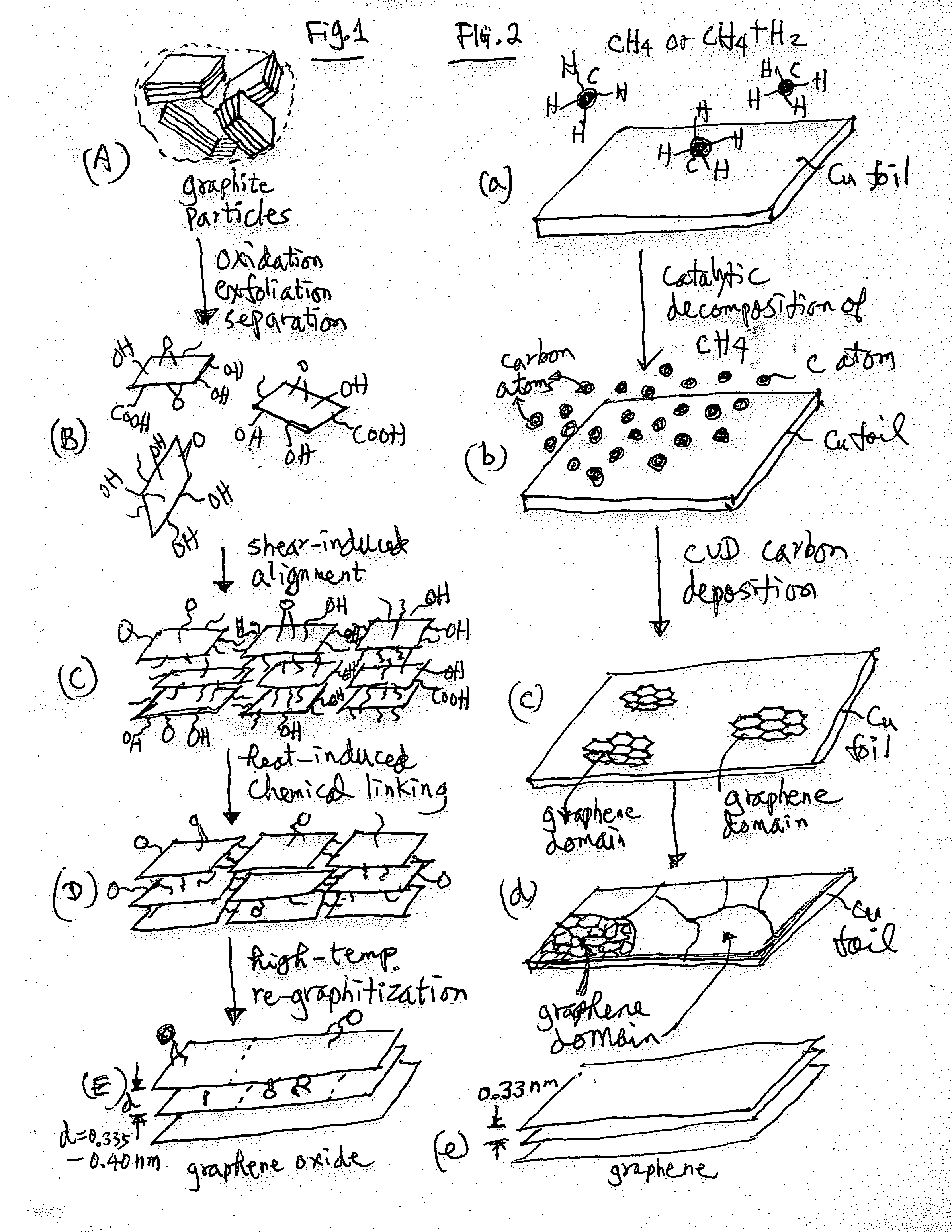
Even with such extreme processing conditions, the resulting PG (including HOPG) still possesses many defects, grain boundaries, and mis-orientations (neighboring graphene planes not parallel to each other), resulting in less-than-satisfactory in-plane properties.
Typically, the best prepared HOPG sheet or block remains far from being a graphite single crystal; instead, it typically still contains many grains or single crystals and a vast amount of grain boundaries and defects.
However, these polycrystalline graphene films are not sufficiently thermally conducting (too many grains or too much grain boundaries, and all grains being oriented in different directions) and not sufficiently thick for use as a heat spreader in an electronic device.

Method used


Image

  • Unitary graphene layer or graphene single crystal
  • Unitary graphene layer or graphene single crystal
  • Unitary graphene layer or graphene single crystal

Examples


example 1

Preparation of Nano Graphene Platelets (NGPs)

[0137]Chopped graphite fibers with an average diameter of 12 μm was used as a starting material, which was immersed in a mixture of concentrated sulfuric acid, nitric acid, and potassium permanganate (as the chemical intercalate and oxidizer) to prepare graphite intercalation compounds (GICs). The fiber segments were first dried in a vacuum oven for 24 h at 80° C. Then, a mixture of concentrated sulfuric acid, fuming nitric acid, and potassium permanganate (at a weight ratio of 4:1:0.05) was slowly added, under appropriate cooling and stirring, to a three-neck flask containing fiber segments. After 16 hours of reaction, the acid-treated graphite fibers were filtered and washed thoroughly with deionized water until the pH level of the solution reached 6. After being dried at 100° C. overnight, the resulting graphite intercalation compound (GIC) was subjected to a thermal shock at 1050° C. for 45 seconds in a tube furnace to form exfoliated...

example 2

Preparation of Single-Layer Graphene from Meso-Carbon Micro-Beads (MCMBs)

[0138]Meso-carbon microbeads (MCMBs) were supplied from China Steel Chemical Co. This material has a density of about 2.24 g / cm3 with a median particle size of about 16 μm. MCMB (10 grams) were intercalated with an acid solution (sulfuric acid, nitric acid, and potassium permanganate at a ratio of 4:1:0.05) for 72 hours. Upon completion of the reaction, the mixture was poured into deionized water and filtered. The intercalated MCMBs were repeatedly washed in a 5% solution of HCl to remove most of the sulphate ions. The sample was then washed repeatedly with deionized water until the pH of the filtrate was neutral. The slurry was dried and stored in a vacuum oven at 60° C. for 24 hours. The dried powder sample was placed in a quartz tube and inserted into a horizontal tube furnace pre-set at a desired temperature, 1,080° C. for 45 seconds to obtain a graphene material. TEM and atomic force microscopic studies in...

example 3

Preparation of Pristine Graphene

[0139]In a typical procedure, five grams of graphite flakes, ground to approximately 20 μm or less in sizes, were dispersed in 1,000 mL of deionized water (containing 0.1% by weight of a dispersing agent, Zonyl® FSO from DuPont) to obtain a suspension. An ultrasonic energy level of 85 W (Branson 5450 Ultrasonicator) was used for exfoliation, separation, and size reduction of graphene sheets for a period of 15 minutes to 2 hours.


PUM

PropertyMeasurementUnit
Temperatureaaaaaaaaaa

Abstract

A unitary graphene layer or graphene single crystal containing closely packed and chemically bonded parallel graphene planes having an inter-graphene plane spacing of 0.335 to 0.40 nm and an oxygen content of 0.01% to 10% by weight, which unitary graphene layer or graphene single crystal is obtained from heat-treating a graphene oxide gel at a temperature higher than 100° C., wherein the average mis-orientation angle between two graphene planes is less than 10 degrees, more typically less than 5 degrees. The molecules in the graphene oxide gel, upon drying and heat-treating, are chemically interconnected and integrated into a unitary graphene entity containing no discrete graphite flake or graphene platelet. This graphene monolith exhibits a combination of exceptional thermal conductivity, electrical conductivity, mechanical strength, surface smoothness, surface hardness, and scratch resistance unmatched by any thin-film material of comparable thickness range.

Description

[0001]The present invention claims the benefits of the following co-pending patent applications:A. Zhamu, et al., “Graphene Oxide Gel Bonded Graphene Composite Films and Processes for Producing Same,” U.S. patent application Ser. No. 13 / 385,813 (Mar. 8, 2012).A. Zhamu, et al., “Graphene Oxide-Coated Graphitic Foil and Processes for Producing Same,” U.S. patent application Ser. No. 13 / 694,161 (Nov. 2, 2012).A. Zhamu, et al., “Thermal Management System Containing a Graphene Oxide-Coated Graphitic Foil Laminate for Electronic Device Application,” U.S. patent application Ser. No. 13 / 694,162 (Nov. 2, 2012).FIELD OF THE INVENTION[0002]The present invention relates generally to the field of graphitic materials for heat dissipation applications, and more particularly to a graphene oxide-derived graphene monolith or graphene single crystal that exhibits a combination of an exceptionally high thermal conductivity, high electrical conductivity, high mechanical strength, good surface scratch re...

Claims


Application Information

Patent Timeline
IPC IPC(8): C01B31/04C30B1/02
CPCC01B31/043C30B1/02B82Y30/00C30B5/00C30B29/02C30B29/68B82Y40/00C01B32/22C01B32/225C01B32/23C01B32/182C01B32/184C01B32/19C01B32/192Y10T428/30Y10S977/734Y10S977/842C01B32/198C01P2006/10C01P2006/32C01P2006/40C01P2006/80
Inventor ZHAMU, ARUNAWANG, MINGCHAOXIONG, WEIJANG, BOR Z.
Owner GLOBAL GRAPHENE GRP INC
Learn More