Non-vacuum method of manufacturing light-absorbing materials for solar cell application

a technology of solar cells and light-absorbing materials, which is applied in the direction of coatings, surface reaction electrolytic coatings, semiconductor devices, etc., can solve the problems of high cost, high cost, and high cost of deposition techniques (e.g. evaporation and sputtering), and achieve good conversion efficiency and simplified fabrication of light-absorbing layers.

Active Publication Date: 2014-09-11
NANO & ADVANCED MATERIALS INST
View PDF4 Cites 8 Cited by
  • Summary
  • Abstract
  • Description
  • Claims
  • Application Information

AI Technical Summary

Benefits of technology

[0007]Disclosed in the present invention is a method of preparing a CZTS-based light absorbing semiconductor for solar cell application. Not only the fabrication of the light absorption layers can be simplified in the manufacturing process, scale up into large substrate with good conversion efficiency can be easily achieved due to ease of control of film thickness and uniformity.

Problems solved by technology

However, the supply of the rare earth metal indium for the CIGS production can be a problem in the near future.
For the methods described above, either expensive deposition techniques (e.g. evaporation and sputtering) or highly toxic and flammable chemicals (e.g. hydrazine) are used in the fabrication processes.
In industrial scale production, the use of high-temperature and high-vacuum equipment will increase the cost as well as the energy consumption.
Besides, the use of large amount of toxic chemicals is detrimental to the environment.
However, the use of highly toxic H2Se gas in CZTS manufacturing process is generally not recommended in large scale production purpose.
However, the method is designed only for a small substrate, and cannot be directly scaled up as a complicated sealing and annealing process under controlled-vacuum conditions is needed.
The problems of the method disclosed in '790 include: selenization requires long time during the disclosed Se annealing step; selenium attacks the substrate and causes an increase in surface roughness during long-time selenization.

Method used


Image

  • Non-vacuum method of manufacturing light-absorbing materials for solar cell application
  • Non-vacuum method of manufacturing light-absorbing materials for solar cell application
  • Non-vacuum method of manufacturing light-absorbing materials for solar cell application

Examples


example 1

Formation of Cu—Zn—Sn Alloy by Single-Bath Formulation

[0038]In this example, a Cu—Zn—Sn alloy is prepared by a single-bath formulation containing a plating composition. An exemplary plating composition is provided in Table 1.

TABLE 1UpperLowerPlating parameterUnitLimitLimitPlatingMain bathSalts of Citrate (include sodium citrate,mM100500Compositionpotassium citrate, mono- / di- / tri- basic)Cu salt (e.g. CuCl2, CuSO4, Cu(NO2)2)mM1050Sn salt (e.g. SnCl2, SnSO4, Sn(NO2)2)mM540Zn salt (e.g. ZnCl2, ZnSO4, Zn(NO2)2)mM50300AdditivesSurfactant (e.g. Sodium dodecyl sulfateg / L110(SDS), N,N-Dimethyl-N-dodecylglycine betaine (EMPIGEN ®BB), Polyethylene glycol (PEG))Aldehyde based compounds (e.g.g / L0.14propenal, aromatic aldehyde,benzaldehyde, formaldehyde)

[0039]Besides the ionic compounds of copper, zinc and tin, the plating composition also includes salts of citrate to stabilize the plating solution and additives such as surfactant and aldehyde based compounds to reduce the surface roughness. Opti...

example 2

Sequential Sulfurization and Selenization of Cu—Zn—Sn Alloy

[0042]An annealing step is required to transform a Cu—Zn—Sn alloy to CZTS light absorbing layer. Annealing conditions for sulfurization and selenization are illustrated in Table 2:

TABLE 2UpperLowerParametersUnitLimitLimitSulfurizationTemperature° C.350600Durationmin30200Ramp rate° C. / min0.22SelenizationTemperature° C.300550Durationmin230Ramp rate° C. / min0.53

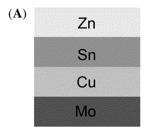
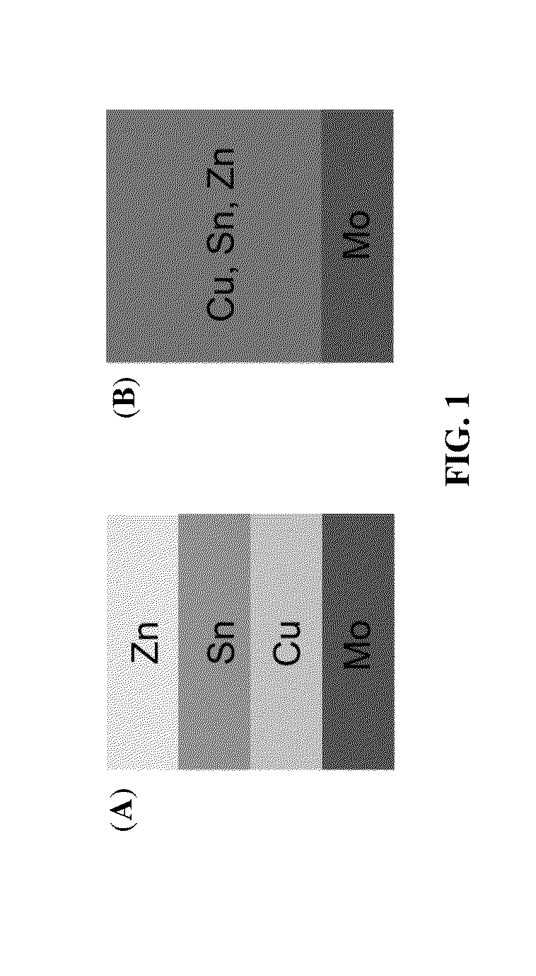
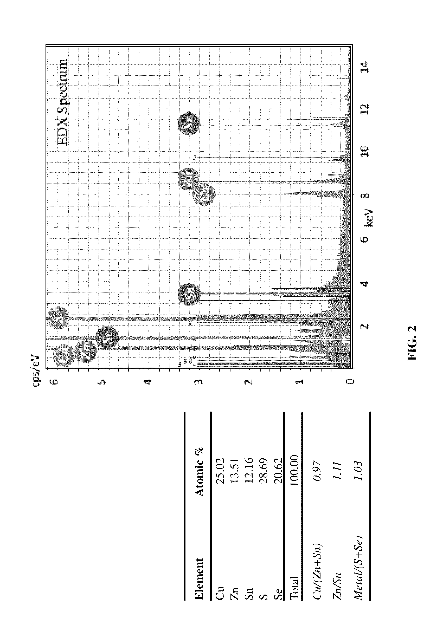
[0043]Flow diagram from formation of Cu—Zn—Sn alloy to annealing is shown in FIG. 4: 401: Formation of Cu—Zn—Sn alloy by co-plating of a single-bath formulation on molybdenum (Mo) substrate; 402: Formation of sulfur-rich atmosphere by using inert carrier gas flowing over sulfur; 403: Formation of Cu—Zn—Sn—S alloy after first annealing; 404: Formation of selenium-rich atmosphere by using inert carrier gas flowing over selenium; 405: Formation of Cu—Zn—Sn—S—Se alloy after second annealing. A schematic diagram summarizing the sequential sulfurization and selenization on the ...

example 3

Formation of Selenium Layer on Alloy Substrate

[0044]It is preferable to electroplate a selenium layer before annealing any alloy substrates under selenium-rich atmosphere. An exemplary plating composition for electroplating the selenium layer is provided in Table 3.

TABLE 3UpperLowerPlating parameterUnitLimitLimitPlatingMain bathMetra-alkyl-quaternary ammonium salt%2060Composition(e.g. choline chloride, betaine, acetylcholine chloride, methyl triphenylphosphunium bromide,tetrabutyl ammonium chloride)Selenium compounds (e.g. seleniummM5100tetrachloride, selenium dioxide,selenium sulfide, selenium oxychloride,selenous acid, and selenic acid)AdditivesSurfactant (e.g. Sodium dodecyl sulfateg / L0.54(SDS), N,N-Dimethyl-N-dodecylglycine betaine (EMPIGEN ®BB), Polyethylene glycol (PEG))Aldehyde based compounds (e.g.g / L0.52propenal, aromatic aldehyde,benzaldehyde, formaldehyde)

[0045]A solvent containing one or more than one kind of tetra-alkyl-quaternary ammonium salt as the major component, a...


PUM

PropertyMeasurementUnit
pHaaaaaaaaaa
temperatureaaaaaaaaaa
pHaaaaaaaaaa

Abstract

The present invention describes a method of producing a p-type light-absorbing semiconductor copper zinc tin selenide/sulfide (Cu2(ZnxSn2-x)(SySe1-y)4) (abbreviated CZTS) with electrochemical deposition. It can be used in the production of solar cell when combined with an n-type inorganic or an organic semiconductor layer. The present method comprises a one-step or a sequence of depositions using electroplating to fabricate a low-cost and large-area CZTS solar cell, without using expensive and complicated deposition techniques or highly toxic and flammable chemicals in the production process. The present method significantly reduces the cost and energy requirement for production of solar cell.

Description

CROSS-REFERENCE TO RELATED APPLICATIONS[0001]The present application claims priority from the U.S. provisional application Ser. No. 61 / 851,407 filed Mar. 7, 2013, and the disclosure of which is incorporated herein by reference in its entirety.FIELD OF THE INVENTION[0002]The present invention relates to a method of producing light-absorbing materials useful for solar cell. In particular, the present invention provides a method of producing a p-type light-absorbing semiconductor based on copper zinc tin selenide / sulfide (Cu2(ZnxSn2-x)(SySe1-y)4) (abbreviated “CZTS”) by using electrochemical deposition, which can be used in the production of solar cell when combined with an n-type inorganic or an organic semiconductor layer. The present invention also relates to a light-absorbing semiconductor prepared by the method of the present invention.BACKGROUND OF THE INVENTION[0003]a-Si, CdTe and CIGS solar cells are being investigated worldwide as new generation thin-film solar cells to succee...

Claims


Application Information

Patent Timeline
Patent Type & Authority Applications(United States)
IPC IPC(8): H01L31/18C25D3/56C25D3/30C25D3/22C25D3/38H01L31/032C25D3/54
CPCH01L31/18H01L31/0326C25D3/56C25D3/30C25D3/22C25D3/38C25D3/54C25D3/565C25D3/58C25D3/60C25D5/10C25D5/50C25D5/505C25D5/611Y02E10/50
Inventor HO, KAM PIUHO, PAUL KWOK KEUNGLIU, MAN WAHWANG, RANSHILUK, WAI CHUNCHOI, WING HOZHENG, FULINKWOK, KWONG CHAUHSU, MEI MEILAU, IVAN KA YU
Owner NANO & ADVANCED MATERIALS INST
Why Eureka
Try Eureka