Method for producing a dielectric and/or barrier layer or multilayer on a substrate, and device for implementing said method

a technology of dielectric and/or barrier layer, applied in the direction of final product manufacturing, chemical vapor deposition coating, climate sustainability, etc., can solve the problem of monolithic integration of metal substrates, inability to make monolithic integration on metal substrates, lack of effective dielectric materials,

Inactive Publication Date: 2015-11-12
ABENGOA SOLAR NEW TECH SA
View PDF0 Cites 5 Cited by
  • Summary
  • Abstract
  • Description
  • Claims
  • Application Information

AI Technical Summary

Problems solved by technology

The development of dielectric and barrier layers for electrically insulating metal substrates or semiconductors is a problem of great significance that determines both the development of electronic circuits smaller in size, as well as, on another level, the industrial development of optoelectronic uses on these types of materials.
Indeed, currently there are no thin-film commercial photovoltaic modules on metal substrates that make use of the monolithic integration technique for the interconnection of solar cells.
One of the reasons for this is the lack of dielectric materials that achieve effective insulation of the metal substrate of the rear electrode of the cell.
In these conditions, monolithic integration cannot be made on a metal substrate due to the development of short circuits between the metal substrate and said rear electrode of the cell.
However, this process does not make use of the active area of the module; it limits the penetration of the product within the architectural market on account of aesthetic aspects, and does not differentiate the product from the conventional Silicio technology, in addition to involving high costs.
However, these metal layers do not have any function of electric insulation preventing the charge migration to the metal substrate; therefore, it is not possible to establish a monolithic integration of the cells in the module.
In these products, the interconnection of cells is performed by conventional welding methods such as mono or polycrystalline silicon technology, which implies disadvantages as a result of having less useful area in the module, as are less power in the module (reduced efficiency), lower production rate, implying higher selling costs of the final product and, furthermore, that does not result in an appealing product for the BIPV (Building Integra

Method used


Image

  • Method for producing a dielectric and/or barrier layer or multilayer on a substrate, and device for implementing said method
  • Method for producing a dielectric and/or barrier layer or multilayer on a substrate, and device for implementing said method
  • Method for producing a dielectric and/or barrier layer or multilayer on a substrate, and device for implementing said method

Examples


example 1

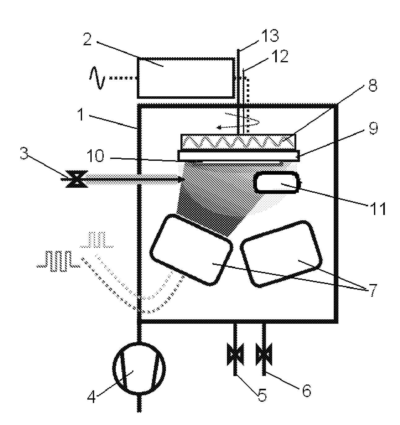
[0070]The following describes in detail an example (Example 1) of the procedure for depositing a layer of silicon dioxide (SiO2) on a metal substrate from a silicon target placed on the cathode of the magnetron, wherein said process includes a deposition stage implementing the PECVD technique, another deposition stage implementing the PVD and PECVD techniques simultaneously, and a final deposition stage applying the PVD technique (sputtering):

[0071]1. The first stage consists in cleaning the substrate (9) by washing it with an aqueous phase, organic or combined solvents, and ultrasound. These are standard pretreatment processes in the industry of coatings on metal substrates and are fully described according to the type of material and the previously performed formation and thermal treatment processes.

[0072]2. The clean and dry substrate (9) is placed on a rotating and polarizable sample holder (8) with a diameter of 10 cm, which is introduced into the vacuum chamber. Cleaning is pe...

example 2

[0082]The following describes in detail an example (Example 2) of the procedure followed to deposit a multilayer system on a metal substrate, where said process includes a deposition stage of SiO2 implementing the PECVD technique, another deposition stage of a mixed oxide of aluminum and silicon (AlxSiyOz), by implementing the PVD and PECVD techniques simultaneously, and a final deposition stage of aluminum oxide (Al2O3), implementing the PVD technique (sputtering).

[0083]1. The first stage consists in cleaning the substrate (9) by washing it with an aqueous phase, organic or combined solvents, and ultrasound. These are standard pretreatment processes in the industry of coatings on metal substrates and are fully described according to the type of material and the previously performed formation and thermal treatment processes.

[0084]2. The clean and dry substrate (9) is placed on a rotating and polarizable sample holder (8) with a diameter of 10 cm, which is introduced into the vacuum ...


PUM

PropertyMeasurementUnit
Temperatureaaaaaaaaaa
Thicknessaaaaaaaaaa

Abstract

The present invention relates to the procedure for the preparation of barrier and/or dielectric layers on a substrate, characterized in that it comprises the following stages: (a) cleaning the substrate, (b) placing the substrate on a sample holder and the introduction thereof into a vacuum chamber, (c) dosage of said vacuum chamber with an inert gas and a reactive gas, (d) injection into the vacuum chamber of a volatile precursor that has at least one cation of the compound to be deposited, (e) activation of a radio frequency source and activation of at least one magnetron, (f) decomposition of the volatile precursor using plasma, the reaction between the cation of the volatile precursor and the reactive gas occurring at the same time that the reaction between the reactive gas contained in the plasma and the cation from the target by sputtering takes place, thus leading to the deposition of the film onto the substrate. The device for carrying out said method is also object of the invention.

Description

TECHNICAL SECTOR OF THE INVENTION[0001]The present invention falls within the field of preparation of thin films having a barrier / dielectric layer effect, with a wide variety of uses. The invention proposed can be especially used in the microelectronic and optoelectronic sectors, primarily in the manufacturing of large-area devices. Within the optoelectronic field, a clear example of usage of the present invention can be found in the design and manufacturing of thin-film photovoltaic solar modules on metal substrates, where the concept of monolithic integration is put into effect for the interconnection of solar cells, and where the development of thin dielectric layers that in addition act as diffusion barriers, is indispensable.[0002]Generally, the present invention can be used in electronics where it is necessary to electrically insulate two metals by means of an intermediate layer that exerts electric insulation and diffusion barrier functions.BACKGROUND OF THE INVENTION[0003]Th...

Claims


Application Information

Patent Timeline
IPC IPC(8): H01J37/34C04B35/44C23C14/35C01B33/12H01L21/02H01L31/0203
CPCH01J37/3473H01L21/02145H01L21/02164H01L21/02178H01L21/02266H01J2237/3323H01J37/3405C23C14/354C01B33/12C04B35/44H01L31/0203H01L21/02274H01L21/022C23C14/0057C23C14/081C23C14/10C23C14/3435C23C14/35C23C16/401C23C16/403C23C16/509H01L31/03926H01L31/03928Y02E10/541Y02P70/50C23C16/40H01J37/34
Inventor GIL ROSTRA, JORGERICO GAVIRA, VICTORYUBERO VALENCIA, FRANCISCOESPINOS MANZORRO, JUAN PEDRORODRIGUEZ GONZALEZ-ELIPE, AGUSTINS NCHEZ CORTEZON, EMILIODELGADO S NCHEZ, JOSE MARIA
Owner ABENGOA SOLAR NEW TECH SA
Why Eureka
Try Eureka