

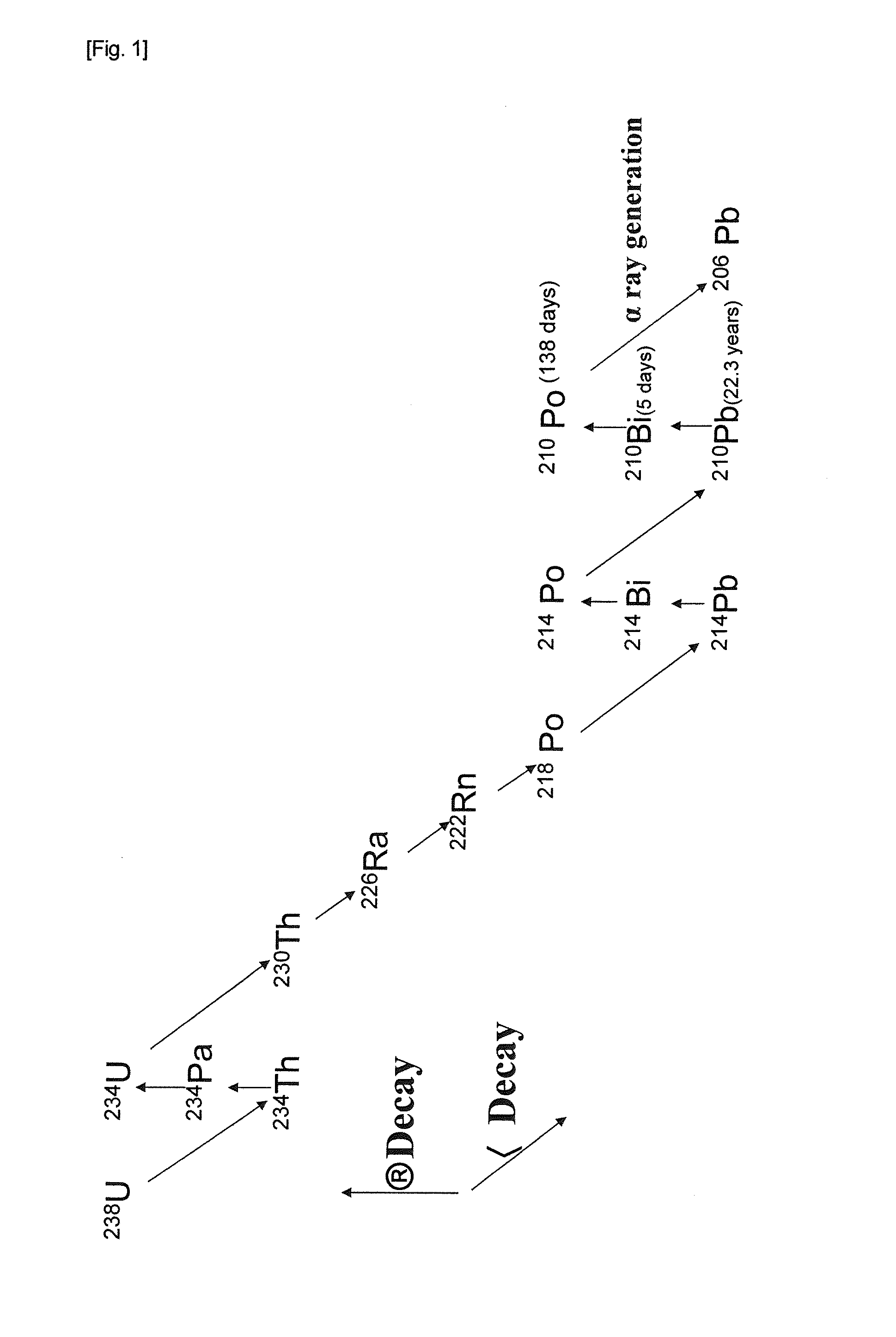
Method of producing low alpha-ray emitting bismuth, and low alpha-ray emitting bismuth
a technology of alpha-rays and bismuth, which is applied in the direction of electrical equipment, solid-state devices, metal-working equipment, etc., can solve the problems of reduced increased risk of soft errors, and high cost of indium, so as to reduce operating voltage and cell volume, the effect of increasing the risk of soft errors
- Summary
- Abstract
- Description
- Claims
- Application Information
AI Technical Summary
Benefits of technology
Problems solved by technology
Method used
Image

Examples
example 1
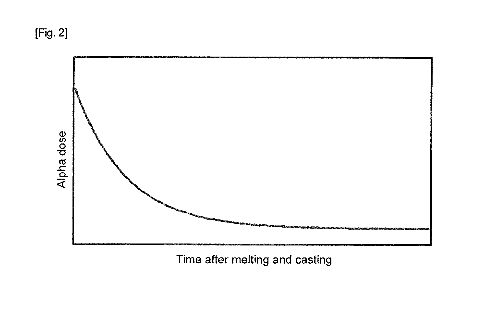
[0080]Raw material bismuth having an alpha dose of 0.483 cph / cm2 was melted in a nitric acid solution via electrolysis to eliminate elements having an electric potential nobler than bismuth. As the bismuth nitrate solution, 100 L of a solution having a Bi concentration of 40.2 g / L and a pH of 0.3 was used.
[0081]The bismuth nitrate solution was passed through, at a rate of 5 L / h, a column filled with 2L of cation-exchange resin of DIAION SK-1 B manufactured by Mitsubishi Chemical Corporation, which is one type of strongly acidic cation-exchange resin and has a sulfonate group (-SO3H) as the exchange group.
[0082]Subsequently, electrowinning was performed at 25 A and 0.48 A / cm2 using the aforementioned solution (filtrate) 1, which was passed through the cation-exchange resin, to eliminate elements having an electric potential baser than bismuth and obtain metal bismuth.
[0083]The alpha dose of the obtained metal bismuth was thereafter measured using an alpha ray measurement device. The ...
example 2
[0085]Raw material bismuth having an alpha dose of 0.462 cph / cm2 was melted in a nitric acid solution via electrolysis to eliminate elements having an electric potential nobler than bismuth. As the bismuth nitrate solution, 100 L of a solution having a Bi concentration of 41.6 g / L and a pH of 0.3 was used.
[0086]The bismuth nitrate solution was passed through, at a rate of 8 L / h, a column filled with 500 mL of cation-exchange resin of DIAION SK-1 B manufactured by Mitsubishi Chemical Corporation.
[0087]Subsequently, electrowinning was performed at 50 A and 0.97 A / cm2 using the aforementioned filtrate 2 to eliminate elements having an electric potential baser than bismuth and obtain metal bismuth.
[0088]The alpha dose of the obtained metal bismuth was thereafter measured using an alpha ray measurement device. The alpha dose of the raw material bismuth and the alpha dose of the refined bismuth are shown in Table 2.
[0089]As shown in Table 2, while the surface alpha dose of the raw materia...
example 3
[0101]2 kg of low alpha-ray emitting bismuth having an alpha dose of 0.003 cph / cm2 which was refined with the method described in Example 1, and 2 kg of tin having an alpha dose of 0.0008 cph / cm2 were filled in a graphite crucible, and the bismuth and tin were alloyed by being mixed and melted at 300° C.
[0102]The alpha dose of the bismuth-tin alloy that was alloyed in Example 3 was 0.0018 cph / cm2, and a bismuth-tin alloy having a low alpha dose was obtained.
[0103]It has been confirmed that, as a material for use in semiconductor chips which are recently of high density and with reduced operating voltage and cell volume, the bismuth-tin alloy having a low alpha dose produced as described above is effective in reducing the occurrence of soft errors caused by alpha rays, and the alpha dose has been reduced to a favorable level as a semiconductor material.
TABLE 5Surface alpha dose(cph / cm2)Refined Bi raw material0.003Refined Sn raw material0.0008Bi—Sn alloy0.0018
PUM
| Property | Measurement | Unit |
|---|---|---|
| pH | aaaaa | aaaaa |
| concentration | aaaaa | aaaaa |
| volume | aaaaa | aaaaa |
Abstract
Description
Claims
Application Information