Method for processing wide-bandgap semiconductor substrate and apparatus therefor

a technology of wide-bandgap semiconductor and processing method, which is applied in the direction of electrical apparatus, semiconductor devices, basic electric elements, etc., can solve the problems of unstable supply of cerium, high cost of treating a polishing liquid, and damage to the surface, so as to promote hydrolysis of oxide film, promote hydrolysis of workpiece, and excellent compatibility with a clean room

Active Publication Date: 2017-03-09
OSAKA UNIV +1
View PDF1 Cites 7 Cited by
  • Summary
  • Abstract
  • Description
  • Claims
  • Application Information

AI Technical Summary

Benefits of technology

[0021]The processing method for a wide-bandgap semiconductor substrate according to the present invention described above is a processing method in which a single crystal, which is SiC, GaN, AlGaN, or AlN, is a work piece, and a surface of the work piece is planarized or processed into an arbitrary curved surface using no abrasive grain or no abrasive. The processing method includes: using a catalytic substance having a function of promoting direct hydrolysis of the work piece or promoting hydrolysis of an oxide film on the surface of the work piece as a processing reference plane; in presence of water, bringing the work piece into contact with or extremely close to the processing reference plane at a predetermined pressure and relatively moving the work piece and the processing reference plane to each other; by a catalyst function of the processing reference plane, advancing a process of direct hydrolysis of the surface of the work piece or a process of oxidation of the surface of the work piece and hydrolysis of the oxide film in priority from a projection on the surface close to the processing reference plane; and removing a decomposition product. Thus, the method can planarize or process the work piece into an arbitrary curved surface. The method has an excellent compatibility with a clean room. The method is easily applied to the fabrication steps of semiconductor devices. The present invention is chemical processing. Thus, the surface of the Si substrate can be processed, without introducing any affected layers. No abrasives or no abrasive grains are used at all on the processed surface. Thus, the surface roughness can be extremely made small, and a surface of higher quality than the quality of a surface finished by CMP can be obtained. Moreover, in the present invention, no chemical agents or no fine particles difficult to be handled, including hydrogen fluoride and other chemical agents, are used. Thus, waste liquids can be extremely easily processed, leading to an advantage in which work environments are greatly improved, although the present invention is a processing method with a small environmental burden. Moreover, no rare earth elements are used at all. Thus, the present invention is not affected by raw material market conditions, allowing running costs to be greatly decreased. In addition, in the present invention, the processing speed is easily controlled, and it is unnecessary to change processing liquids in order to change processes from coarse polishing to precise polishing unlike CMP.
[0022]A potential control unit is included in the processing reference plane having a conductive catalytic substance at least on its surface, the potential control unit controlling processing speed by changing a potential of the catalytic substance. A potential of the processing reference plane is set in a range of ±1 V relative to an oxygen production potential. In this setting, conditions can be set, in which the surface oxidation of a wide-bandgap semiconductor substrate, such as SiC and GaN, which are hard-to-work materials, can be promoted, allowing a great increase in the processing speed. Controllin

Problems solved by technology

However, previously existing CMP uses hard diamond abrasive grains, and thus, the surface is damaged.
However, because producer countries of cerium, which is a rare earth element, are unevenly distributed, the stable supply of cerium has a geopolitical risk.
In addition, CMP uses fine particles, such as colloidal silica, causing problems, such as expensive costs in treating a polishing liquid and poor compatibility of fine particles with a clean room.
However, CARE uses a processing liquid, to which molecules containing halogen are dissolved, specifically a hydrogen fluoride solution, causing necessities of the airtightness of processing spaces and processing facilities for exhaust gas and waste liquids.
Thus, there are problems that costs of handling and apparatus are more increased than in CMP.
However

Method used


Image

  • Method for processing wide-bandgap semiconductor substrate and apparatus therefor
  • Method for processing wide-bandgap semiconductor substrate and apparatus therefor
  • Method for processing wide-bandgap semiconductor substrate and apparatus therefor

Examples


example 1

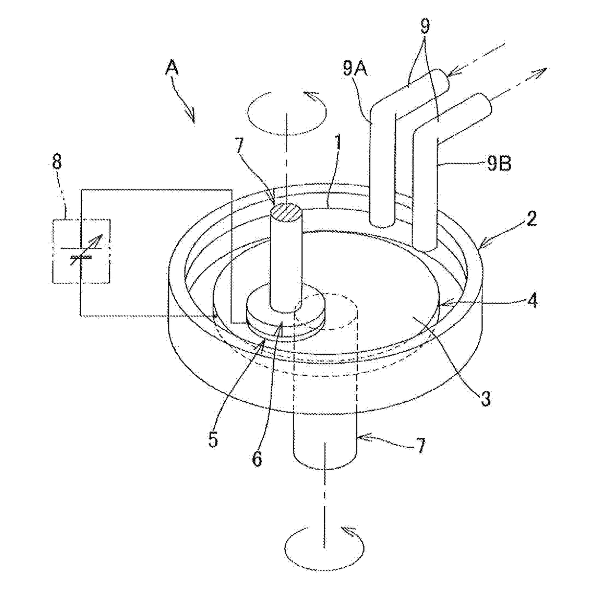
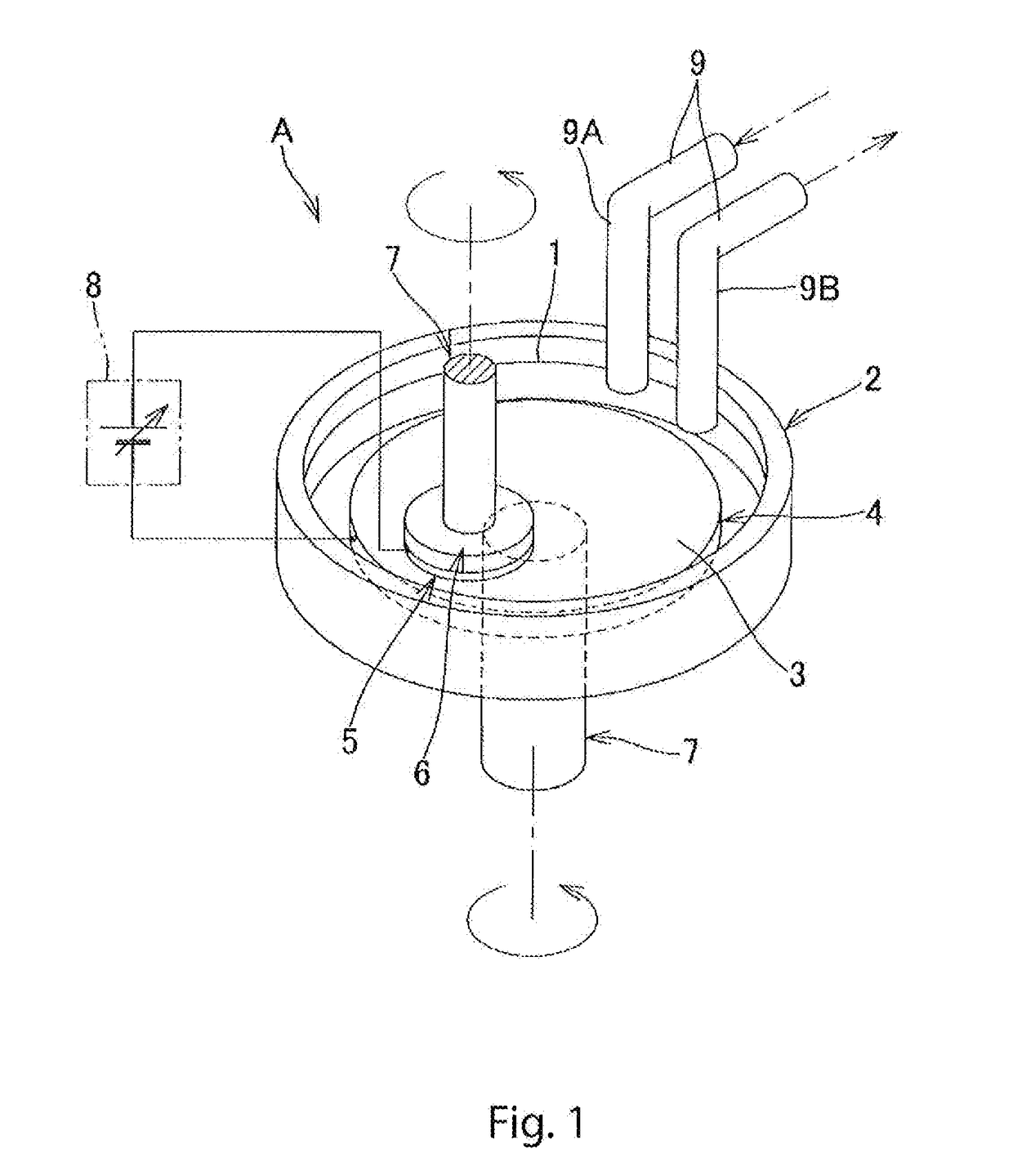
[0067]Next, FIGS. 4 to 9 show the result of experimentally processing of SiC and GaN by the processing apparatus A using Pt as a catalytic substance forming a processing reference plane. For the processing reference plane, a rubber pad was used, in which a Pt film in a thickness of 100 nm was formed on the surface of the rubber pad, and the rubber pad was held on the surface of the rotating platen. The potential of the catalyst was not adjusted and processing was all performed at a rest potential. Surfaces before and after planarization were observed using a phase shift interference microscope (NewView made by Zygo Corporation) and an atomic force microscope (AFM), and the processing characteristics were evaluated.

[0068]FIG. 4 shows experimental processing using a two-inch n-type 4H—SiC (0001) on-axis wafer. In the processing conditions, the catalyst was Pt, the processing liquid was ultrapure water, the processing pressure was 400 hPa, and the rotational speed was 10 rpm. FIG. 4(a)...

example 2

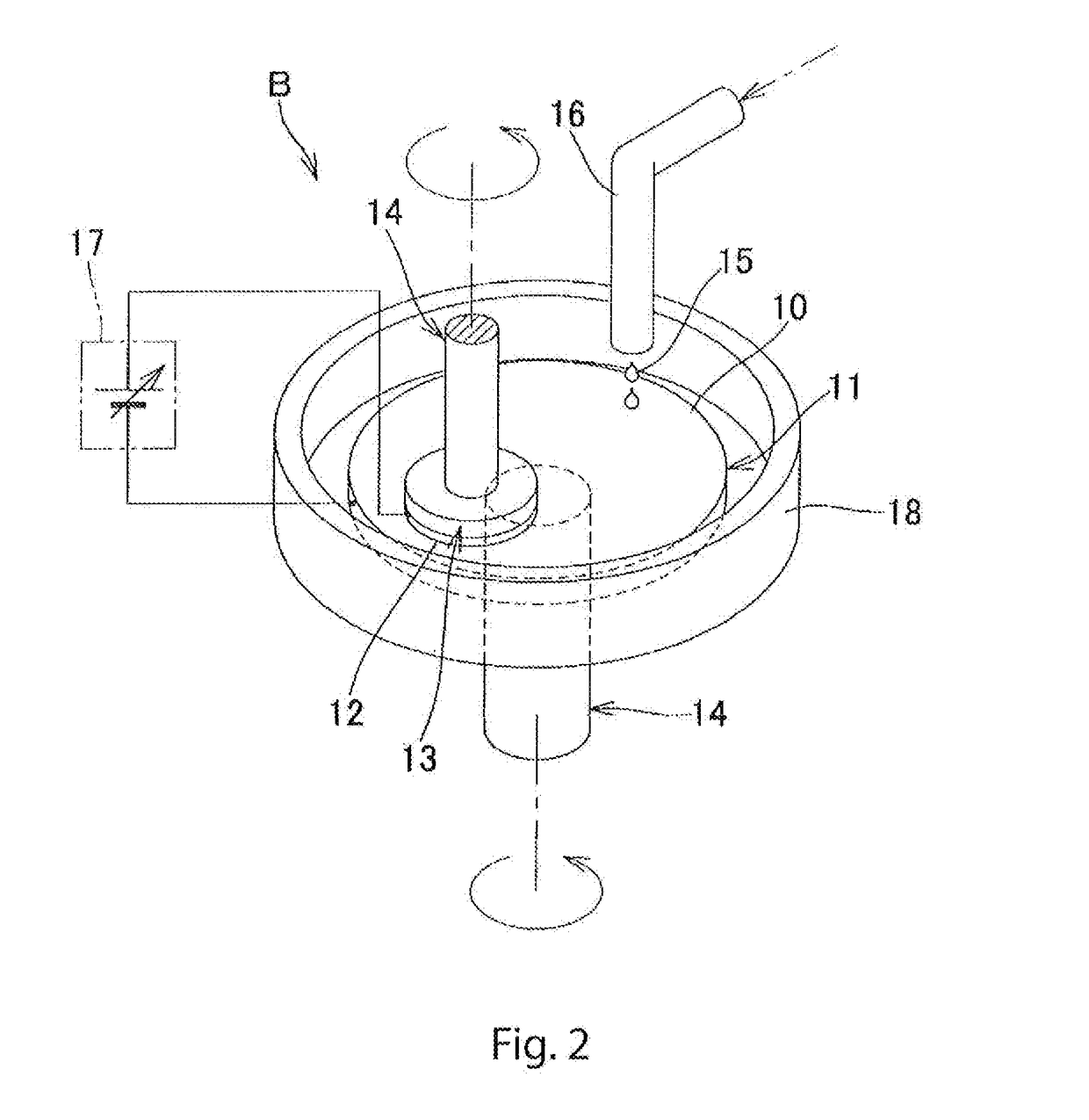
[0076]Next, the controllability of processing speed was checked using the local processing apparatus C. First, the dependence of the processing speed on the processing pressure and the dependence of the processing speed on the rotational speed were checked using a 4H—SiC substrate. FIG. 11 shows the dependence on the processing pressure. FIG. 12 shows the dependence on the rotational speed. The dependence on the processing pressure was checked under the processing conditions in which the catalyst was Pt, the processing liquid was pure water, the processing pressure was 100 to 1,000 hPa, and the rotational speed was 10 rpm. The dependence on the rotational speed was checked under the processing conditions in which the catalyst was Pt, the processing liquid was pure water, the processing pressure was 400 hPa, and the rotational speed was 5 to 25 rpm. The potential of Pt is a rest potential. Only an elliptic region, with which Pt was brought into contact, was processed. The maximum dep...

example 3

[0093]Lastly, the dependence of the processing speed on a catalyst was checked using catalytic substance balls 36 formed with various catalytic metals. A processing target is a 4H—SiC (0001) wafer. In the processing conditions, the catalysts were various metals, the processing liquid was pure water, the contact pressure was 2,000 hPa, and the rotational speed was 24 rpm. The potential of the catalytic metal was a rest potential. For a catalytic metal, Ni, Pt, Cu, and Au were tested. Each of the catalytic metals was formed in a film on the surface of a rubber ring by sputtering vapor deposition. The result is shown in FIG. 21.

[0094]Ni achieves the processing speed 13 times the processing speed of Pt. It can be considered that the processing speed can be further improved depending on the selection of catalytic substances. Also in GaN (0001), a similar tendency was observed in the dependence of the catalytic metal on the processing speed. In the present invention, water is basically us...


PUM


Abstract

There are provided a processing method for a wide-bandgap semiconductor substrate and an apparatus therefor that use no abrasives or no abrasive grains, or no solution having a large environmental burden at all, can process a single crystal, which is SiC, GaN, AlGaN, or AlN, at a variety of processing speed, can obtain a surface of higher quality than the quality of a surface finished by CMP, and also have an excellent compatibility with a clean room. A catalytic substance having a function of promoting the direct hydrolysis of a work piece (5) or promoting the hydrolysis of an oxide film on the surface of the work piece is used as a processing reference plane (3). In the presence of water (1), the work piece is brought into contact with or extremely close to the processing reference plane at a predetermined pressure.

Description

TECHNICAL FIELD[0001]The present invention relates to a method for processing a wide-bandgap semiconductor substrate and an apparatus therefor, and more specifically to a processing method that can process a wide-bandgap semiconductor substrate, such as an SiC substrate and a GaN substrate, with a decreased environmental burden and an apparatus therefor.BACKGROUND ART[0002]Conventionally, in the field of manufacture of semiconductor devices, there are provided various methods of planarizing or polishing the surface of an Si substrate including Si wafers in high quality. Typically, there is CMP (Chemical Mechanical Polishing). In recent years, as a new technique of processing a hard-to-work material, such as SiC, and a solid oxide film, such as optical glass, CARE (CAtalyst-Referred Etching) has been proposed.[0003]CMP is a technique, in which by a surface chemical action caused by an abrasive (an abrasive grain) or by the action of chemical components contained in a polishing liquid...

Claims


Application Information

Patent Timeline
IPC IPC(8): H01L21/306H01L21/04
CPCH01L21/30612H01L21/30625H01L21/30604H01L21/0445H01L21/02019H01L21/0475H01L21/302H01L21/32134H01L21/67086H01L29/1608
Inventor YAMAUCHI, KAZUTOISOHASHI, AISANO, YASUHISA
Owner OSAKA UNIV
Why Eureka
Try Eureka