Batch-processing method for super-high aspect ratio diffractive optics

a diffractive optic and super-high aspect ratio technology, applied in the field of batch processing of high-aspect ratio diffractive optic devices, can solve the problems of insufficient x-ray or particle beam focusing efficiency, the modest aspect ratio of the features that all these types of lithography and methods are capable of producing, and the inability to manufacture self-standing geometric objects of this aspect ratio without collapse or distortion, etc., to achieve the effect of reducing the cost of production

Active Publication Date: 2017-09-07
ALCORIX CO
View PDF1 Cites 18 Cited by
  • Summary
  • Abstract
  • Description
  • Claims
  • Application Information

AI Technical Summary

Benefits of technology

[0056]For example, a preferred embodiment of a method for fabricating Fresnel zone plates disclosed herein overcomes at least some disadvantages of the conventional ALD-and-slice method, by replacing wires or hollow tubes with arrays of a plurality of precursor forms, e.g. cylindrical columns or cylindrical holes, or cylindrical columns within cylindrical holes, etched in a planar substrate, such as a silicon wafer. Using cylindrical columns to deposit the sequential layers around them has the advantage of enabling a better characterization of the side wall roughness and tilt of the columns versus cylindrical holes. Using cylindrical columns within concentric cylindrical holes provides a surrounding region of the substrate which confers robustness to the column structures for withstanding mechanical polishing. Formation of precursor structures and deposition of sequential layers by ALD is followed by standard batch-processing methods, to replace the conventional tedious serial slicing and individual wire polishing processes with mature and rapid wafer-level processing. This approach allows for parallel processing of hundreds of devices at a time at the wafer level, with processes common through-out the electronics and MEMS industry. The limitations of the disclosed process reside primarily in the accuracy of producing the initial precursor structures (e.g. cylindrical columns, cylindrical columns within cylindrical holes, or other precursor forms or precursor structures disclosed herein) and in controlling the thicknesses in the sequenced layer deposition, practically, in the 1 nm to 100 nm range. The innovative process sequence allows for device thicknesses limited in practice primarily by the fabrication process height limits of columns and holes in semiconductor substrates, which are typically in the range from a fraction of a μm to hundreds of μm. This translates into potential aspect ratios for the resulting zone plate lines of up to tens of thousands or even hundreds of thousands to one.
[0057]For example, the focussing efficiency of the resulting diffractive optic comprising a zone plate depends on factors including the aspect ratio, the amount of phase shift, which is preferably π, or close to π, provided between adjacent zones, and the quality of the execution of the zone plate structure. Smoothing of sidewalls of the precursor forms prior to deposition of the sequence of layers of the diffractive line pattern improves the quality of execution of the diffractive line patterns. That is, since any initial roughness or non-uniformity of surfaces of the precursor forms are propagated in successively deposited layers, smoothing of surfaces of the precursor form allows for closer control of the thickness and uniformity of the deposited sequence of layers forming the specified diffractive line pattern of the zone plate.

Problems solved by technology

Self-standing geometric objects of this aspect ratio are essentially impossible to fabricate without collapse or distortion at this time.
The limitations of all these types of lithography and methods are the modest aspect ratios of the features that they are capable of producing.
These aspect ratios are insufficient for efficient focusing of x-rays, or particle beams of a corresponding energy.
One drawback of this method is the accentuation or amplification of radius irregularities of the central wire (i.e. the roughness or accidental other variations including particulate defects and thickness variations during the deposition) as successive layers are deposited beginning from the bare wire and proceeding to the outermost layer.
A second drawback is the accumulation of the absolute error values of the depositions thicknesses of each of the inward layers as an error of placement of the next outward layer.
Thus, the outermost (i.e. thinnest) layers accumulate the largest radius errors due to the amplification and accumulation of the depositional processes errors through successive layers.
This error amplification process can produce defects in the final (thinnest) zone shape and placement exceeding a half-width of the layer / zone itself, rendering that portion of the diffractive line useless for focusing or adequate manipulation of phase shift of the prescribed photon or particle beam.
However, in order to effectively reduce the error amplification process, the slit widths have to be reduced to fractions of the wire diameter, which reduces the deposition rate to impractically low values.
Another drawback of the sputter-and-slice method is that only one wire can be processed at a time, while the slicing / polishing procedures are serial and time-consuming.
The method suffers from the same drawbacks as the wire-based version and can be used only for linear (one-dimensional) optics; however, it has shown relatively higher rates of success because it is easier to obtain highly planar and smoothly-polished planar surfaces rather than perfectly circular, low roughness wires or tubes.
However, this method still preserves error accumulation in layer thicknesses, but these errors are more easily kept in control, due to the more precise nature of the ALD process.
An additional drawback of the ALD-and-slice method is the relative slow rate of deposition in ALD processes, which require months-long deposition times for Fresnel Zone Plates with a reasonable number of zones.
In practice, for deposition by sputtering, this fabrication process would be limited by the variation of thickness of sputtered layers with the depth in the hole, inherent to the sputtering process.
As mentioned above, while sequential ALD is capable of deposition of conformal layers of uniform and controlled thickness, in practice, the method of Yun et al. would be limited by the surface roughness of the cylindrical holes, which depends on the etch process used for etching the holes.
Thus, the thickness of the thinnest functional zone of the diffractive optic is limited by the average roughness of the side walls, which is usually tens or hundreds of nm for most etching processes.
This accuracy is difficult to characterize in holes of the required depth and aspect ratio, except by destructive procedures.

Method used


Image

  • Batch-processing method for super-high aspect ratio diffractive optics
  • Batch-processing method for super-high aspect ratio diffractive optics
  • Batch-processing method for super-high aspect ratio diffractive optics

Examples


first embodiment

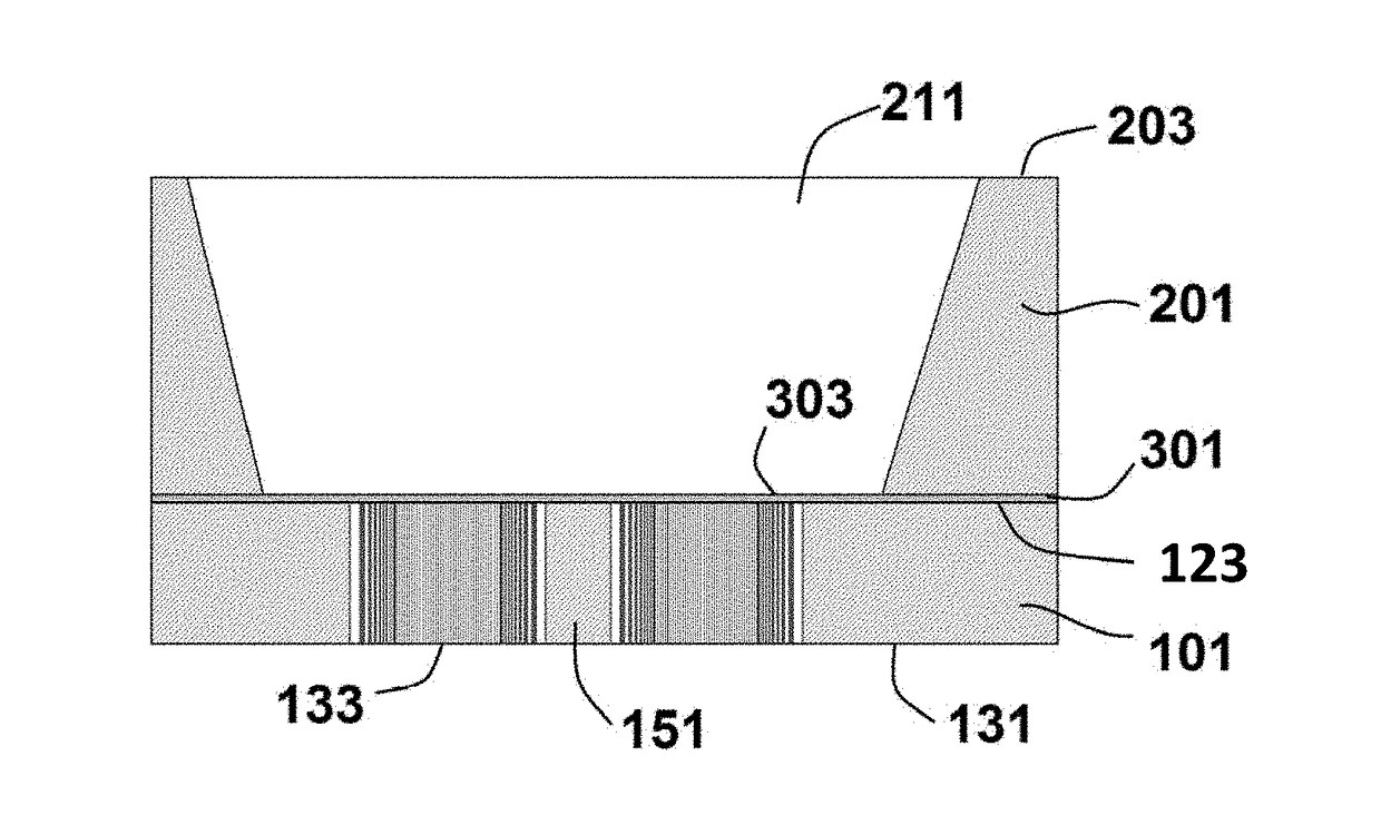
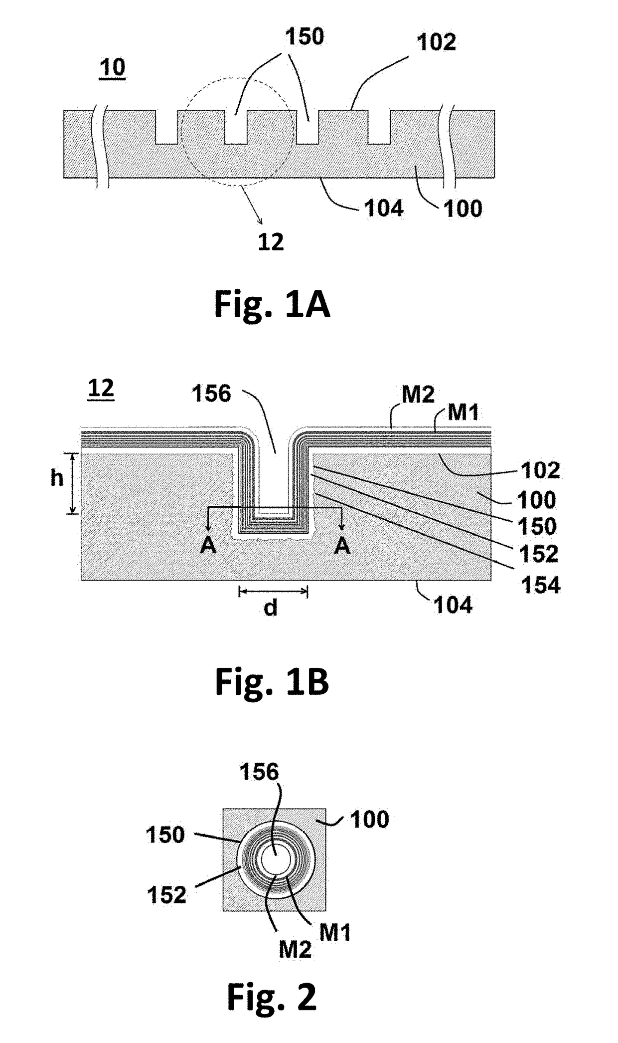
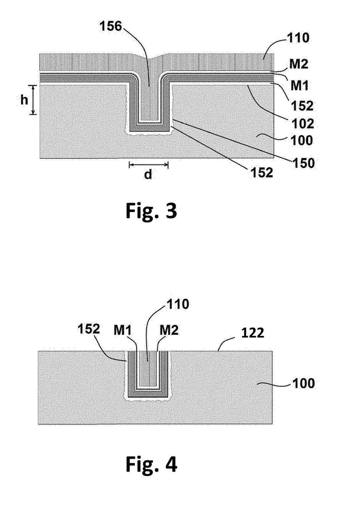
[0084]FIGS. 1A and 1B and FIGS. 2 to 7 illustrate schematically steps in a method of fabricating a device structure comprising a high aspect ratio diffractive optic comprising a Fresnel Zone Plate (FZP). The resulting device structure is shown in FIG. 7.

[0085]FIG. 1A shows a schematic cross-sectional view part of a precursor device structure 10 comprising an array of cylindrical holes 150 defined in a planar substrate 100. The planar substrate comprises, for example a silicon wafer having a smooth polished planar front surface 102 and back surface 104. FIG. 1B shows an enlarged view of part 12 of FIG. 1A, comprising one of the array of cylindrical holes 150, after deposition of a planarization layer 152 and a sequence of conformal layers comprising a first material M1 and a second material M2 have been deposited in the cylindrical hole. As illustrated schematically, there are alternating layers of M1 and M2. The electromagnetic properties of each of first and second materials M1 an...

fourth embodiment

[0119]Thus, FIG. 17A shows a schematic cross-sectional view of a multiple-phase diffractive optics device of a fourth embodiment, comprising a FZP for hard X-rays, using multiple layers (N) stacks of materials M1, M2, . . . MN. FIG. 16B illustrates the resulting N-steps phase shift approximation corresponding to an ideal continuous-varying phase shift in a kinoform as shown in FIG. 16C. Thus, it will be appreciated that the method can be readily generalized for multilayer stacks of ALD films, M1, M2, . . . MN, to approach a smooth variation of absorbance of phase shifting across Fresnel zones, for an increase in efficiency and elimination of unwanted focusing / diffraction orders.

[0120]In the device structures of the embodiments described in detail above, the diffractive optics comprise diffractive line patterns in the form of concentric circular zones, formed within a cylindrical hole or around a cylindrical column or post. By providing a precursor structure or form comprising a plan...

second embodiment

[0125]For example, for a two dimensional diffractive optic, if the precursor form 30 comprises an array of cylindrical columns 351 of the appropriate dimensions for forming FZP similar to those of the second embodiment, the columns in holes are structured for forming arrays of zone plates with at least a minimum distance between them. That is, while the precursor form illustrated in FIG. 8A has one cylindrical column in each cylindrical hole, the precursor form as illustrated in FIG. 18, for forming a two dimensional diffractive optic, comprises a group of a plurality of cylindrical columns 351 formed within each cylindrical hole 350, with islands 352 of the substrate surrounding each hole. The larger islands 352 or reinforcing regions of the substrate around groups of columns provide a more robust substrate structure during fabrication, and e.g. to provide areas of the planar substrate surface that act as a polish stop layer for the chemical-mechanical polishing steps.

[0126]For for...


PUM

PropertyMeasurementUnit
energyaaaaaaaaaa
diameteraaaaaaaaaa
angleaaaaaaaaaa

Abstract

A method for fabrication of diffractive optics by batch processing is disclosed, having applicability to high resolution ultra-high aspect ratio Fresnel Zone Plates for focusing of X-rays or gamma-rays having energies up to hundreds of keV. An array of precursor forms is etched into a planar substrate. Sidewalls of the forms are smoothed to a required surface roughness. A sequence of alternating layers of different complex refractive index, for binary or higher order diffractive optics, are deposited on the precursor forms by atomic layer deposition (ALD), to provide diffractive line patterns. Thinnest layers may have nanometer thicknesses. After front surface planarization and thinning of the substrate to expose first and second surfaces of the diffractive line patterns of the diffractive optic, the height h in the propagation direction provides a designed absorption difference and/or phase shift difference between adjacent diffractive lines. Optionally, post-processing enhances mechanical, thermal, electrical and optical properties.

Description

CROSS REFERENCE TO RELATED APPLICATION[0001]This application claims priority from U.S. Provisional patent application No. 62 / 302,352, filed Mar. 2, 2016, entitled “Batch-Processing Method for Super-High Aspect Ratio Diffractive Optics”, which is incorporated herein by reference in its entirety.FIELD OF THE INVENTION[0002]This invention relates to a method of manufacturing high aspect ratio diffractive optic devices applicable to the focusing or shaping of wave fronts of very high energy electromagnetic radiation or particle beams using curved or variable-spaced diffractive lines of absorber or phase shifter materials, with sub-20 nm features and aspect ratios up to tens of thousands to one.BACKGROUND[0003]Many diffractive optics devices, such as those used for focusing X-rays or particle rays (elementary particles or ions), use high-aspect-ratio or free-standing curved or variable-width line grids, or, they are composed of a succession of absorption or refractive index varying absor...

Claims


Application Information

Patent Timeline
Patent Type & Authority Applications(United States)
IPC IPC(8): G21K1/06B24B37/04C23C16/04B24B7/22C23C16/455C23C16/02
CPCG21K1/062C23C16/45555C23C16/0227G21K2201/067C23C16/0254B24B7/228B24B37/042C23C16/045C23C16/06C23C16/342C23C16/45529G21K1/06Y10S148/05C23C16/042C23C14/042B81C2201/0104H01L21/7684H01L21/32115H01L21/02065H10K71/166
Inventor MOLDOVAN, NICOLAIE A.
Owner ALCORIX CO
Why Eureka
Try Eureka