Polymer-Metal Compound Composite Ink, and Preparation Method and Application Thereof

a technology of metal oxide and composite ink, which is applied in the direction of arsenic oxides/hydroxides/oxyacids, tungsten oxides/hydroxides, etc., can solve the problems of many defects on the surface of thin films, inability to meet ink-based printing, and inability to achieve ink-based printing. , to achieve the effect of easy preparation, low cost and convenient availability of raw materials

Active Publication Date: 2018-01-18
SUZHOU INST OF NANO TECH & NANO BIONICS CHINESE ACEDEMY OF SCI
View PDF1 Cites 11 Cited by
  • Summary
  • Abstract
  • Description
  • Claims
  • Application Information

AI Technical Summary

Benefits of technology

[0026]1) the polymer-metal compound composite ink and the thin film of the present invention are easily available in raw material, easy to prepare and low in cost;
[0027]2) the use of the thin form formed from the polymer-metal compound composite ink of the present invention as interface modification material may improve the film compactness of the interface modification layer, reduce the surface roughness of the interface modification layer and thus improve the performance of the device; for example, when used for electrode interface modification, the thin film may realize the adjustment of a surface work function of electrodes;
[0028]3) the polymer-metal compound composite ink of the present invention may be deposited by spin-coating, blade-coating, ink-jet printing or in other common ways to form a thin film, and thus has the advantages of simple processing process and the like; and
[0029]4) when the polymer-metal compound composite ink of the present invention is used as interface modification material, the performance of the formed device is lowly dependent upon the thickness of the thin film, the process requirements for the preparation of the device can be reduced, and it is advantageous to increase the yield of the device.

Problems solved by technology

However, conventional metal oxide thin films are mostly deposited by vacuum sputtering which is not compatible with ink-based printing.
However, since the nanoparticle disperse liquid is likely to result in aggregation of nanoparticles when printing and preparing a thin film, there are many defects on the surface of the thin film and the thin film is rigid and easy to fracture.
In addition, since the energy band structure of pure metal oxides is determined by a material preparation process and is difficult to adjust in the later stage, the metal oxides are somewhat limited in practical applications.
However, it is difficult to remove the surfactant in the later stage.
If the surface of the organic active layer is treated by plasma or ultraviolet ozone, the equipment is highly required, and it is likely to damage the organic thin film to a certain extent so that the service life of the device is shortened.
However, the methods for synthesizing and preparing such ionic polymer electrolytes based on the conjugated polymer material are complicated and high in material cost.
However, due to the poor electricity conductivity of the polymers, when the polymers are used as an electrode interface modification layer, the device performance is highly dependent upon the thickness of the thin film.
Thus, the preparation process of the device is very difficult.
However, in this method, the aggregation of metal oxide nanoparticles still occurs during the deposition of the first metal oxide thin film.
In addition, the number of electrode modification interfaces is increased, the factors which influence the device performance are also increased, and the preparation process of the device becomes more complicated.
However, such material also has the problems of serious aggregation and high film roughness.

Method used


Image

  • Polymer-Metal Compound Composite Ink, and Preparation Method and Application Thereof
  • Polymer-Metal Compound Composite Ink, and Preparation Method and Application Thereof
  • Polymer-Metal Compound Composite Ink, and Preparation Method and Application Thereof

Examples


embodiment 1

of ZnO:PEI (Zinc Oxide:Polyethyleneimine) Composite Ink and its Application in an Organic Photovoltaic Device

[0130]The specific operation steps of this embodiment are as follows.

[0131]1. Preparation of ZnO nanoparticles: 2.950 g of zinc acetate dehydrate was dissolved into 125 mL of absolute methanol, and then heated to 60 while stirring. 1.480 g of potassium hydroxide was ultrasonically dissolved into 65 mL of absolute methanol, the methanol solution of potassium hydroxide was quickly added into the zinc acetate solution, and the mixture was heated to 60 to 65 and then magnetically stirred for 2 h at 600 rpm. During the reaction, the solution was first colorless and then separated out white precipitate; then, the precipitate disappeared gradually, and the solution became light blue; about 2 h later, white precipitate was separated out; the system was continuously heated for 0.5 h; the heating was stopped, the reaction was completed.

[0132]2. Preparation of ZnO ink: After the ZnO nan...

embodiment 2

[0138]Preparation of ZnO:PEIE composite ink: a ZnO ink (its preparation process may refer to Embodiment 1) having a concentration of 10 mg / mL and a PEIE (80% methoxylatedpolyethylenimine) solution having a weight concentration of 0.4% were mixed at a different volume ratio and ultrasonically dispersed to obtain the ZnO:PEIE composite ink.

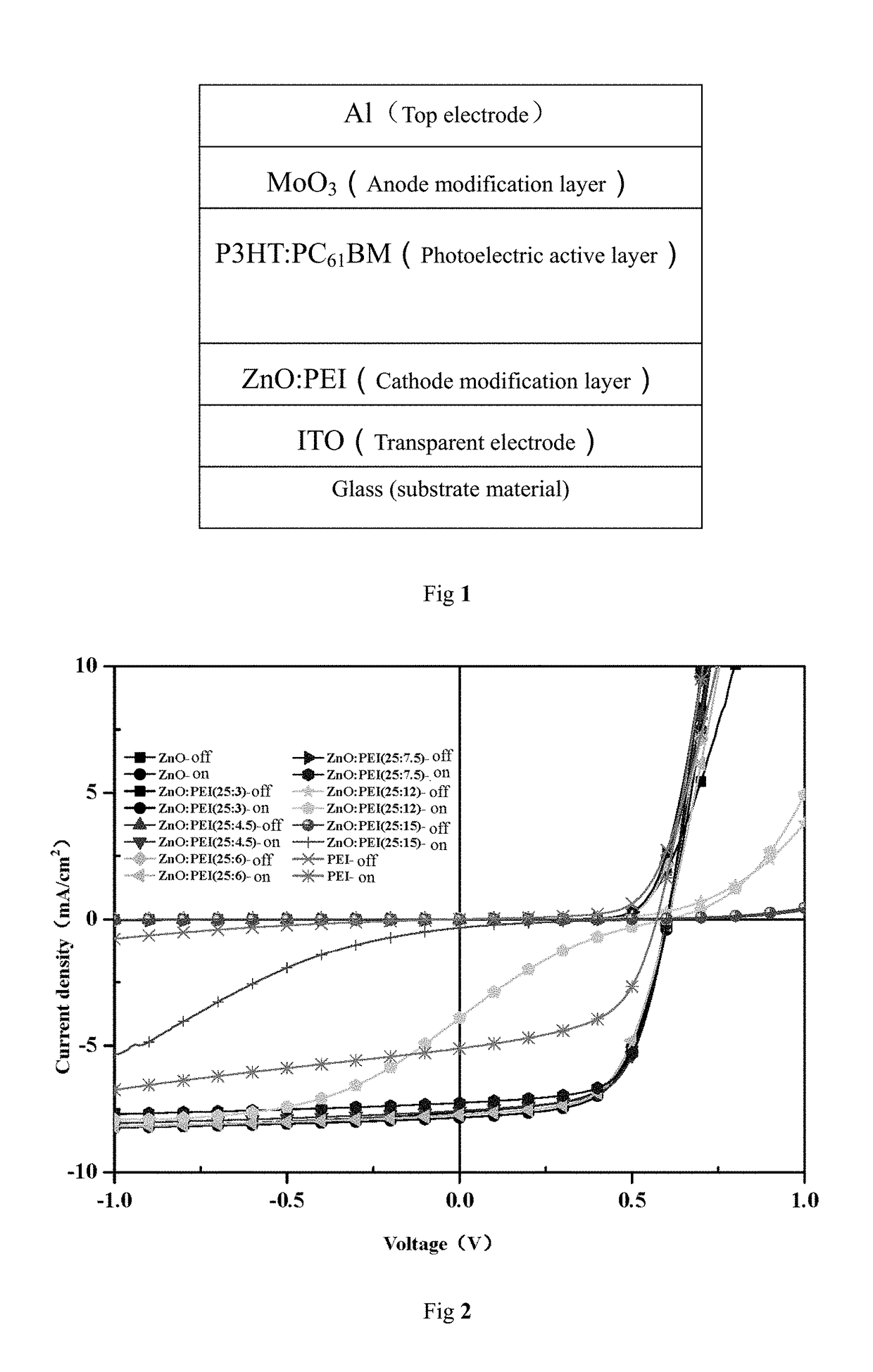
[0139]Preparation of ZnO:PEIE composite cathode modification layer: spin-coating was performed on the ITO surface at 2300 rpm to obtain a ZnO:PEIE composite cathode modification layer.

embodiment 3

of PMA:PEDOT:PSS Composite Ink and its Application in an Organic Photovoltaic Device

[0140]1. The preparation process of the PMA:PEDOT:PSS composite ink includes the following steps.

[0141](1) Preparation of PMA ink: 1 mg of H3PO4.12MoO3.3H2O (PMA) powder was added with 1 mL of redistilled isopropanol, and the mixture was ultrasonically processed to be completely dispersed to obtain the PMA ink having a weight concentration of 1 mg / mL.

[0142](2) Preparation of PMA:PEDOT:PSS composite ink: the PMA ink having a concentration of 1 mg / mL and an PEDOT:PSS (Clevios PV P AI4083) ink were mixed at a different volume ratio and then ultrasonically dispersed to obtain the PMA:PEDOT:PSS composite ink.

[0143]2. The preparation process of a corresponding PMA:PEDOT:PSS composite thin film includes: coating the PMA:PEDOT:PSS composite ink on substrate material by spin-coating, blade-coating or other common methods, and drying to obtain the composite thin film.

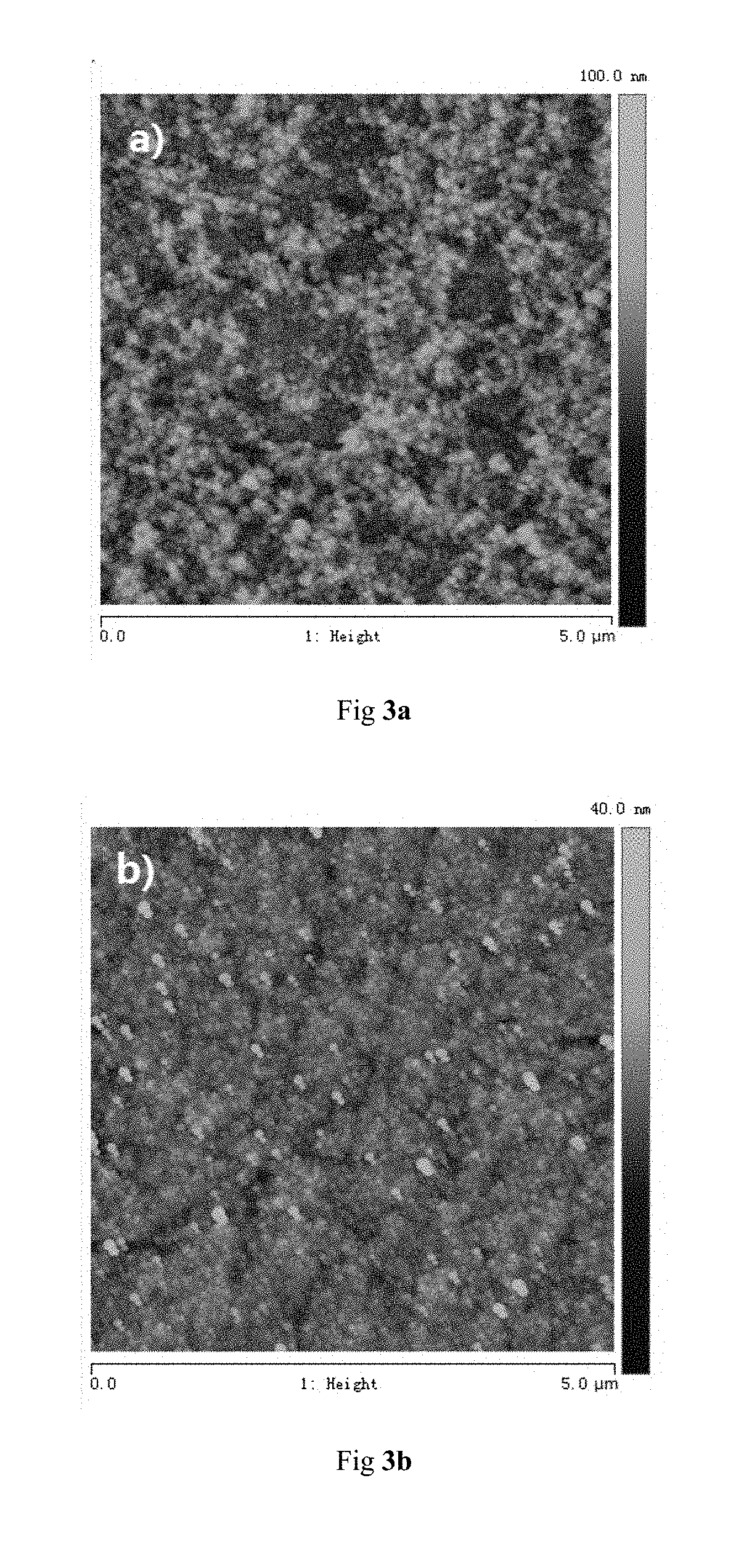
[0144]Characterization results of the PMA:P...


PUM

PropertyMeasurementUnit
concentrationaaaaaaaaaa
particle diameteraaaaaaaaaa

Abstract

The present invention discloses a polymer-metal compound composite ink, a preparation method and application thereof. The composite ink comprises: at least one polymer; at least one metal compound material, the metal compound material being selected from polyoxometalate compounds and nanocrystalline metal oxides; at least one solvent which is used for forming a disperse system in the form of a uniform fluid together with the remaining components in the composite ink. The present invention also discloses a method for preparing the composite ink. The composite ink of the present invention is easily available in raw material, easy to prepare and low in cost, and can be manufactured into a composite thin film by spin-coating, printing or in other ways. The composite thin film, as an electrode modification layer, can be applied to photoelectric devices such as solar cells or light-emitting diodes, so as to improve the contact performance between an electrode and an organic active layer and thus enhance the performance and yield of photoelectric devices.

Description

TECHNICAL FIELD OF THE INVENTION[0001]The present invention particularly relates to a polymer-metal compound composite ink and a preparation method and application thereof, for example, an application in photoelectric devices, belonging to the field of photoelectric semiconductor material and devices.BACKGROUND OF THE INVENTION[0002]Compared with conventional inorganic photoelectric devices, novel solution-processed photoelectric devices based on organic semiconductor material, for example, organic solar cells, perovskite solar cells and Organic Light-Emitting Diodes (OLEDs), have a very broad application prospect due to their advantages of low cost, light and soft properties, convenience for large-scale roll-to-roll production and the like. Such novel photoelectric conversion devices are generally of a sandwich multilayer structure including an active layer and electrodes. The electrodes include a cathode and an anode. Wherein, the electrodes mainly function to complete injection (...

Claims


Application Information

Patent Timeline
Patent Type & Authority Applications(United States)
IPC IPC(8): C09D11/106C09D11/037C09D11/102B82Y40/00C01G17/00C01G28/00C01G31/02C01G39/02C01G41/02C08F12/26C08F226/06H05B33/00
CPCC09D11/106C09D11/102C09D11/037C01G31/02C01G41/02C01G39/02C01G28/005C01G17/00C08F226/06C08F12/26B82Y40/00H05B33/00C08L65/00C08G61/126C08G2261/1424C08G2261/3223C08G2261/794C09D165/00H10K50/15H10K2102/331H10K71/15Y02E10/549
Inventor WANG, YILINGLUO, QUNWU, NAMA, CHANGQI
Owner SUZHOU INST OF NANO TECH & NANO BIONICS CHINESE ACEDEMY OF SCI
Why Eureka
Try Eureka