Fluorine-containing silicon network polymer, insulating coating thereof, and electronic devices therewith

a technology fluorine, which is applied in the direction of electrolysis organic production, coating, electrolysis components, etc., can solve the problems of difficult industrialization, deterioration of throughput, and difficulty in fine patterns, so as to achieve controllable heat stability of silicon network polymer, low thermal resistance of straight chain polysilane, and the effect of low cos

Inactive Publication Date: 2000-01-18
RENESAS ELECTRONICS CORP
View PDF3 Cites 15 Cited by
  • Summary
  • Abstract
  • Description
  • Claims
  • Application Information

AI Technical Summary

Benefits of technology

The inventors applied the same exposing and heating process as above to straight chain polysilane. As a result, there was no polysilane film on the substrate at both the exposed area and the unexposed area, after the heat treatment. The reason lies in that the thermal resistance of straight chain polysilane is low.
The heat stability of the silicon network polymer of the present invention can be controlled by changing the formula ratio of the organic metal compound represented by the formulas 1 and 2 in polymerization reaction. As the formula ratio is increased, the heat stability becomes high. If it is necessary to form no fine pattern, it is possible to abbreviated the exposure process. Even if the silicon network polymer formed by abbreviating the exposure process is thermally treated at 200.degree. C. to 1,000.degree. C. in the presence of oxygen, an insulating film of which the characteristic of electricity is excellent. Further, by oxydizing silicon network polymer without heating it, irradiating light to it in the presence of oxygen, it is possible to obtain an insulating film having an improved characteristic in electricity. If necessary, both the photoreaction and the thermal reaction can be used or either of them can be used. The volume expansion due to oxidation reaction can be controlled according to the stage of the process of the photo-oxidation reaction and the thermal oxidation reaction and according to the stage of the process of the thermal decomposition reaction of the organic group. Finally, it is possible to eliminate the volume expansion of the thin film or occur the volumetric shrinkage.
In case that the formed thin film is applied to a semiconductor device, a mechanical characteristic of the thin film becomes very important. If the film to be formed is shrunken in the process of forming, the tensile stress is generated. Therefore, the formed film is fragile and is apt to crack due to a small external force. While, If the film to be formed is expanded in the process of forming, the compression stress is generated. It is, therefore, hard to crack and extremely advantageous to work the film.
Because the film containing many SiO skeletons according to the present invention can control the volume expansion and the film stress generated as described above, it is optimum to use in the manufacturing process of a semiconductor device. It is desirable that in order to prevent a thin film from cracking, it needs to expand the film in the process of forming, or suppress the amount of shrinkage to the minimum amount. Because the thin film of silicon network polymer according to the present invention is excellent in a coating characteristic and a film characteristic, the thickness of the film to be formed is not limited. If a thin film is formed by using spin coating, it is easiest to obtain a thin film with even thickness of 0.1 .mu.m to 1.0 .mu.m.

Problems solved by technology

Further, because the resolution at the edge of a pattern is small, it is very difficult to form fine patterns.
In addition, because it is necessary to use special-purpose and expensive equipment in order to perform the dry etching, the throughput is deteriorated.
However, since large amounts of organic solvent such as xylene or toluene are used in the wet-etching, and these solvents are flammable and extremely poisonous, it is very difficult to industrialize.

Method used


Image

  • Fluorine-containing silicon network polymer, insulating coating thereof, and electronic devices therewith
  • Fluorine-containing silicon network polymer, insulating coating thereof, and electronic devices therewith
  • Fluorine-containing silicon network polymer, insulating coating thereof, and electronic devices therewith

Examples


embodiment 1

(Embodiment 1)

Tetrahydrafuran solution, 200 ml, of 0.4 mol of tetrachrolosilane and 0.4 mol of pentafluorobromobenzene was dropped into a nitrogen-converted flask provided with a magnesium operation electrode and a pair of nickel electrodes by using a dropping funnel, with ice-cooling. The Grignard reaction of tetrachrolosilane and pentafluorobromobenzene was performed under the circulating flow of solvent.

Reaction was performed at 0.degree. C. during 3 hours, with electric potential scanning at 50 mV / sec between -3 V and 0 V applied between the electrodes. The reacted solution is poured into methanol of 100 ml, and re-precipitated and refined by using distilled water of 500 ml. The yield was 51.3%.

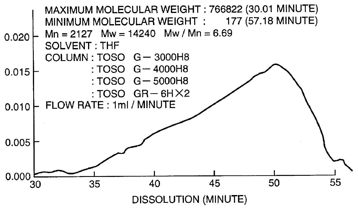
The average molecular weight of polystylene conversion measured by GPC was 14,240.

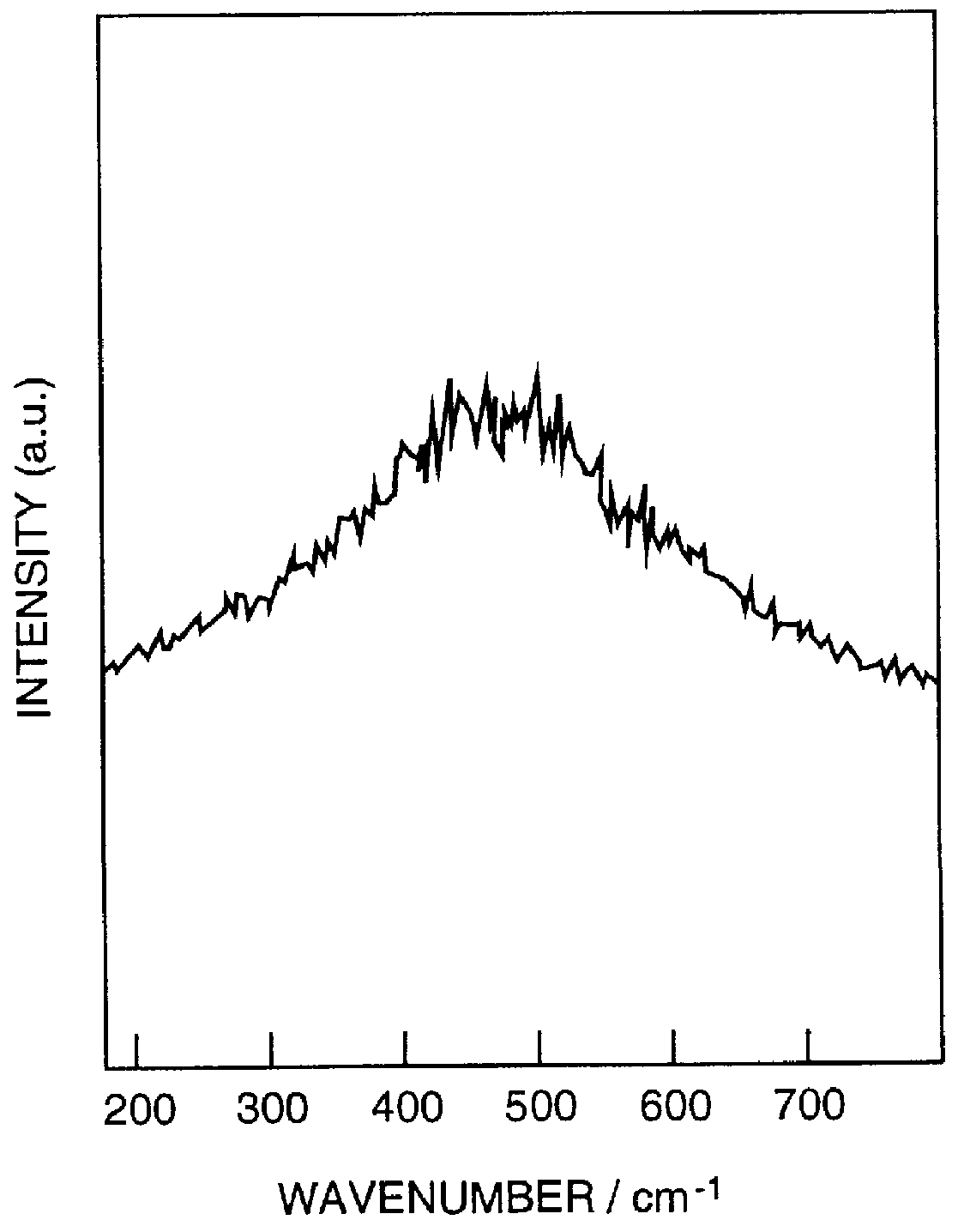
FIG. 1 shows a GPC chart of the obtained poly (pentafluorophenylsilane), and FIG. 2 shows Raman spectrum of the polymer. It is understood that the spectrum of Si--Si bond is broad and networked. The ACS Symp...

embodiment 2

(Embodiment 2)

Pentafluorobromobenzene is changed for nonafluoroiodobutane, and the synthesis is carried out in the same way as Embodiment 1. As a result, poly (nonafluorobutylsilane) was obtained with the yield of 55%.

embodiment 3

(Embodiment 3)

Pentafluorobromobenzene is changed for heptafluoroiodopropane, and the synthesis is carried out in the same way as Embodiment 1. As a result, poly (heptafluoropropylsilane) was obtained with the yield of 50%.


PUM

PropertyMeasurementUnit
wavelengthaaaaaaaaaa
wavelengthsaaaaaaaaaa
temperatureaaaaaaaaaa

Abstract

PCT No. PCT/JP96/01107 Sec. 371 Date Oct. 27, 1997 Sec. 102(e) Date Oct. 27, 1997 PCT Filed Apr. 24, 1996 PCT Pub. No. WO96/34034 PCT Pub. Date Oct. 31, 1996A fluorosilicon network polymer prepared by the reaction of a tetraholosilane of the formula 1: SiX4 with an organohologen compound of the formula 2: RZ , an insulating coating prepared therefrom, semiconductor devices coated therewith, and processes for producing the same. In said formulas, R represents at least monofluorinated alkyl or aryl; and X and Z represent each independently boromine, iodine or chlorine.

Description

The present invention relates to silicon network polymer containing fluorine in polymer structure, an insulating film and a manufacturing method thereof. Further, the present invention relates to a method of forming a thin film by a photolithography method, using silicon network polymer containing fluorine in polymer structure.In the Journal of The Japanese Society of Applied Physics, Volume 34, L452, 1995, there is disclosed silicon network polymer and the synthesizing method thereof. The synthesizing method uses Wurtz's reaction in which trihalosilane is condensation-reacted with sodium metal.Further, in Japanese Patent Application Laid-Open No. 3-258834 (1991), there is disclosed straight chain fluorine-containing polysilane and the synthesizing method thereof. This also uses Wultz's reaction.However, in the prior art, fluorine-containing silicon network polymer has never been synthesized. The reason is that the compounds which can be used for the Wurtz's reaction are limited, an...

Claims


Application Information

Patent Timeline
Patent Type & Authority Patents(United States)
IPC IPC(8): C08G77/00C08G77/60H01L21/02H01L21/316H01L21/312
CPCC08G77/60H01L21/02131H01L21/02164H01L21/02167H01L21/02282H01L21/02337H01L21/02348H01L21/02354H01L21/3121H01L21/31629
Inventor MIWA, TAKAOWATANABE, AKIRAITO, OSAMUMATSUDA, MINORU
Owner RENESAS ELECTRONICS CORP
Why Eureka
Try Eureka