

Method for producing an epitaxial silicon single crystal wafer and the epitaxial silicon single crystal wafer
a single crystal wafer and epitaxial silicon technology, applied in the direction of crystal growth process, polycrystalline material growth, chemistry apparatus and processes, etc., can solve the problems of low productivity, low gettering capability, and low gettering capability compared
- Summary
- Abstract
- Description
- Claims
- Application Information
AI Technical Summary
Benefits of technology
Problems solved by technology
Method used
Image

Examples
example 3
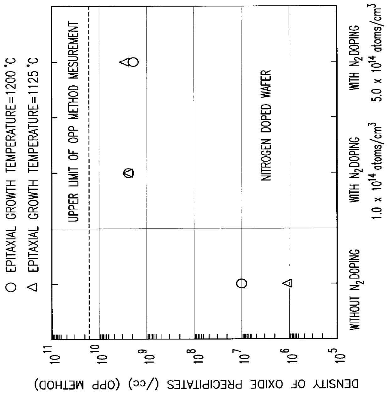
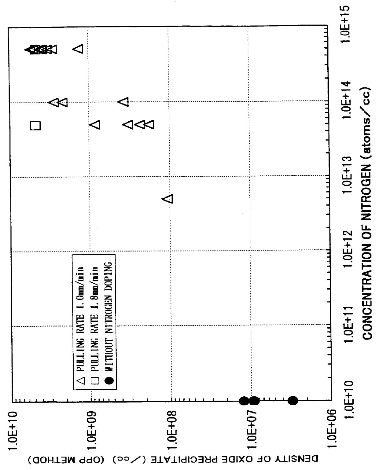
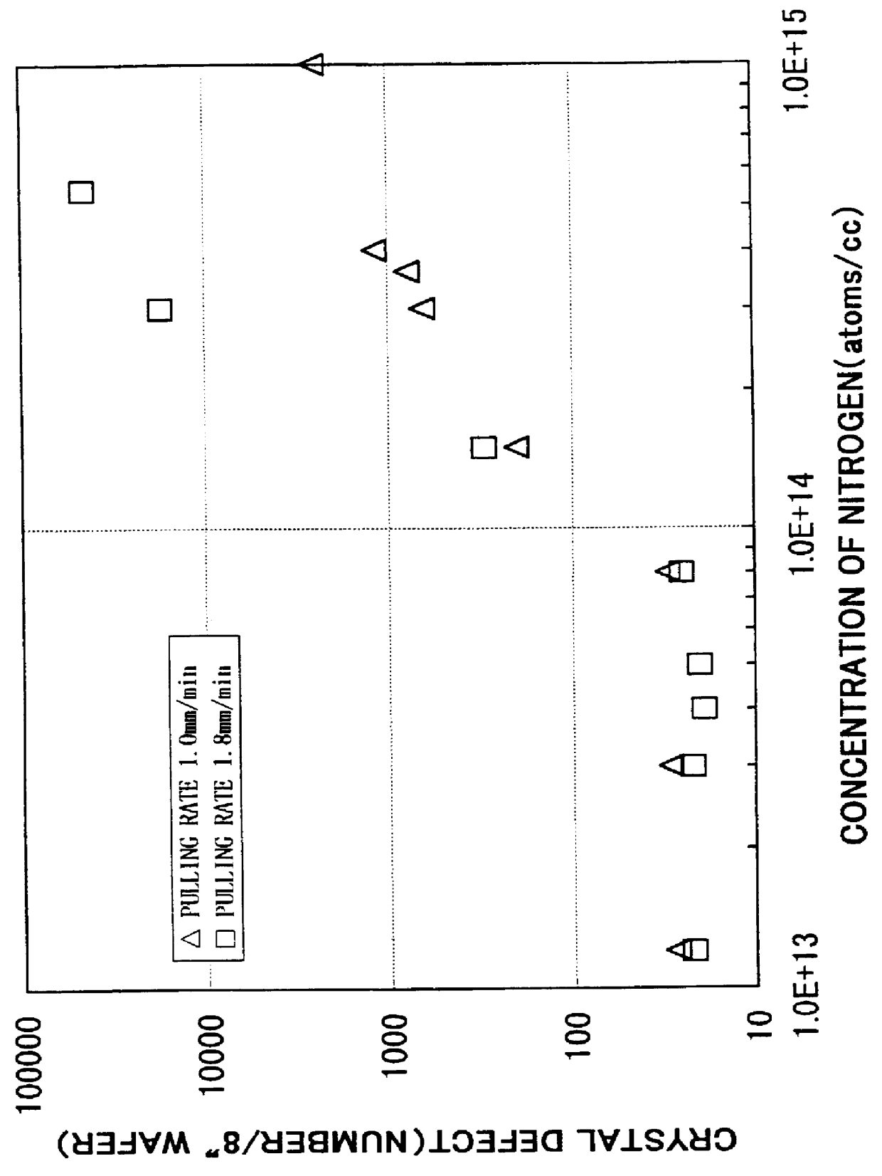
In accordance with CZ method, in a similar way to the method of Example 1, silicon single crystal ingots of p-type (boron doped) having a diameter of 8 inches and orientation were pulled at a pulling rate of 1.0 mm / min and 1.8 mm / min. They were pulled with controlling the amount of a wafer with a silicon nitride film previously charged so that nitrogen concentration may be 1.times.10.sup.13 to about 1.times.10.sup.15 atoms / cm.sup.3. The silicon single crystal mirror wafers having various nitrogen concentration were produced from the resultant single crystal ingots having various nitrogen concentration. Any of the resultant silicon single crystal mirror wafer had resistivity of about 10.OMEGA..multidot.cm and oxygen concentration of 10 to 18 ppma (JEIDA).
Then, hydrogen bake was performed at 1130.degree. C. for one minute, followed by silicon epitaxial growth at 1090.degree. C. to form an epitaxial layer having thickness of 15 .mu.m.
The density of crystal defects such as stacking fau...
example 4
In accordance with CZ method, in a similar way to the method of Example 1, silicon single crystal ingots of p-type (boron doped) having a diameter of 6 inches and orientation were pulled at a pulling rate of 1.0 mm / min. They were pulled with controlling the amount of a wafer with a silicon nitride film previously charged so that nitrogen concentration may be about 5.times.10.sup.4 atoms / cm.sup.3. Any of the resultant silicon single crystal mirror wafer had resistivity of about 10.OMEGA..multidot.cm and oxygen concentration of 16 ppma (JEIDA).
Then, the heat treatment before epitaxial growth was performed through use of SHS-2800 manufactured by Steag Microtech International corporation, RTA (Rapid Thermal Annealing) apparatus which is a lamp heating type apparatus. The heat treatment was performed at 1200.degree. C. for 0 to 3600 seconds in an atmosphere of 25% of H.sub.2 and 75% of Ar. When the heat treatment was performed for more than 60 seconds, it was performed in such way that ...
PUM
| Property | Measurement | Unit |
|---|---|---|
| melting point | aaaaa | aaaaa |
| resistivity | aaaaa | aaaaa |
| size | aaaaa | aaaaa |
Abstract
Description
Claims
Application Information