Optoelectronic device and laser diode

a technology of optoelectronic devices and laser diodes, which is applied in the direction of instruments, semiconductor lasers, optical elements, etc., can solve the problems of increasing the cost of the device, affecting the performance of the device according to the related art, and reducing the yield of the devi

Inactive Publication Date: 2001-12-04
KK TOSHIBA
View PDF6 Cites 27 Cited by
  • Summary
  • Abstract
  • Description
  • Claims
  • Application Information

AI Technical Summary

Problems solved by technology

Like the above, in the laser diode having an optical waveguide structure according to the related art, a number of manufacturing steps are needed since the device requires a complicated structure.
Especially, there are problems such that its yield becomes lower and its cost increases higher because a plurality of delicate manufacturing procedures like the epitaxial crystal growth have reliability problems at regrowth interfaces.
In addition, in the device structure in the related art, restrictions are imposed upon design of the optical waveguide and the electrode, and therefore it is difficult to improve the performance of the device according to the related art.
Also, crystal properties are damaged if the dry etching is applied to the semiconductor crystal, nevertheless the transparent electrode is less damaged by the dry etching because it is not formed of a single crystal.

Method used


Image

  • Optoelectronic device and laser diode
  • Optoelectronic device and laser diode
  • Optoelectronic device and laser diode

Examples


embodiment 1

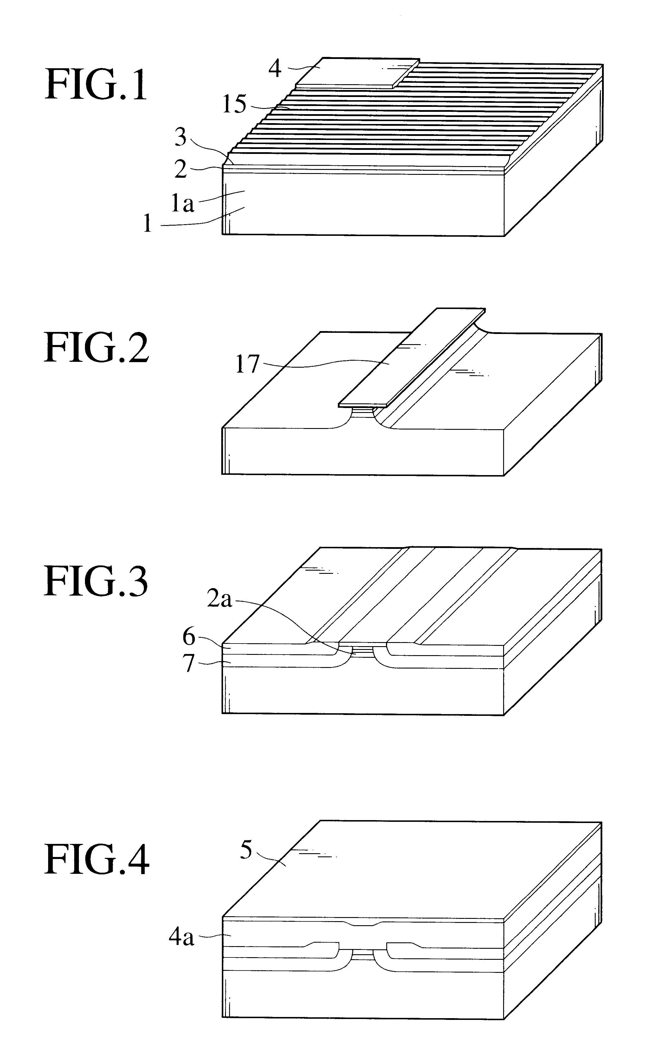
FIGS. 7A and 7B are schematic perspective views showing a structure of a laser diode according to a first embodiment of the present invention respectively. To begin with, as shown in FIG. 7A, an n-InP substrate 1 (including an n-InP buffer layer 1a), an MQW active layer 2, a p-InP layer 4, and a p-InGaAsP waveguide layer 3 are grown in sequence. Differences from the related art in FIG. 1 reside in that the p-InP layer 4 of 0.3 .mu.m (preferably 0.05 .mu.m to 0.7 .mu.m, and more preferably 0.1 .mu.m to 0.5 .mu.m) thickness is grown on the MQW active layer 2 to constitute a double-hetero structure and then the waveguide layer 3 of 0.2 .mu.m (preferably 0.02 .mu.m to 0.5 .mu.m, and more preferably 0.05 .mu.m to 0.3 .mu.m) thickness is grown on the p-InP layer 4. The crystal growth must be effected only once at this time.

Then, a diffraction grating 15 is formed thereon. A number of steps are prepared after this step in the related art. But, in this example, as shown in FIG. 7B, only an ...

embodiment 2

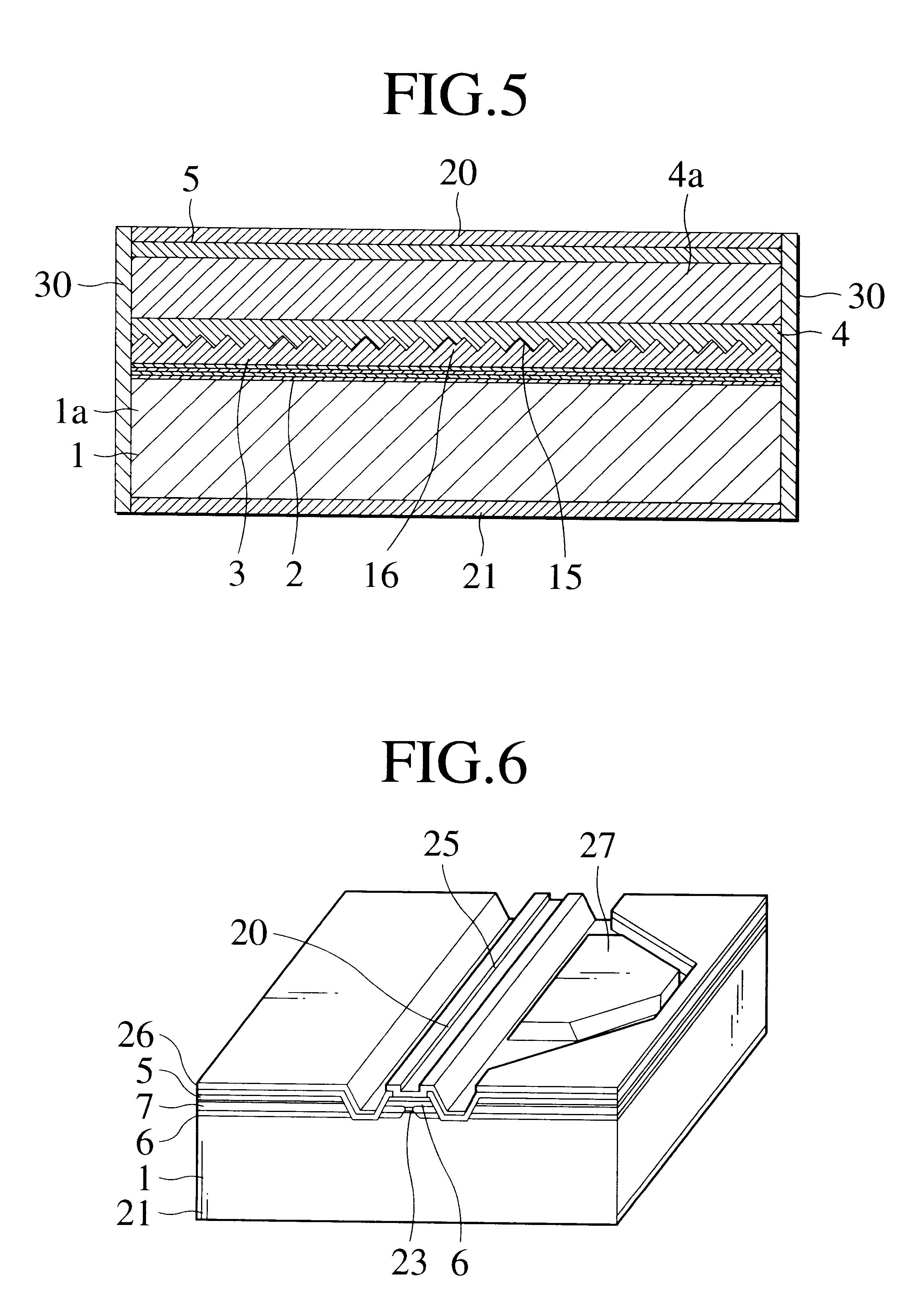
The DFB laser is constructed by using the diffraction grating formed on the semiconductor in the first embodiment and the related art, but transparent electrode itself can also be designed to perform a function of the diffraction grating. In this case, since there is no need of forming the diffraction grating on the epitaxially grown semiconductor, manufacture of the device becomes much easier. In particular, if a selective etching process only for transparent electrode material is employed to remove the electrode, manufacturing steps subsequent to the transparent electrode can be tried again without loss of the expensive semiconductor layer structure just in case of troubles. In addition, since, unlike the epitaxial growth, there is no necessity of matching the lattice constant to the semiconductor substrate, margin in design such as control of the refractive index, insertion of an insulating film, etc. can be increased. Further, the device can be free from the masstransport phenom...

embodiment 3

An embodiment in which the present invention is not applied to control of the longitudinal mode in the DFB laser but to control of the transverse mode will be explained hereinbelow.

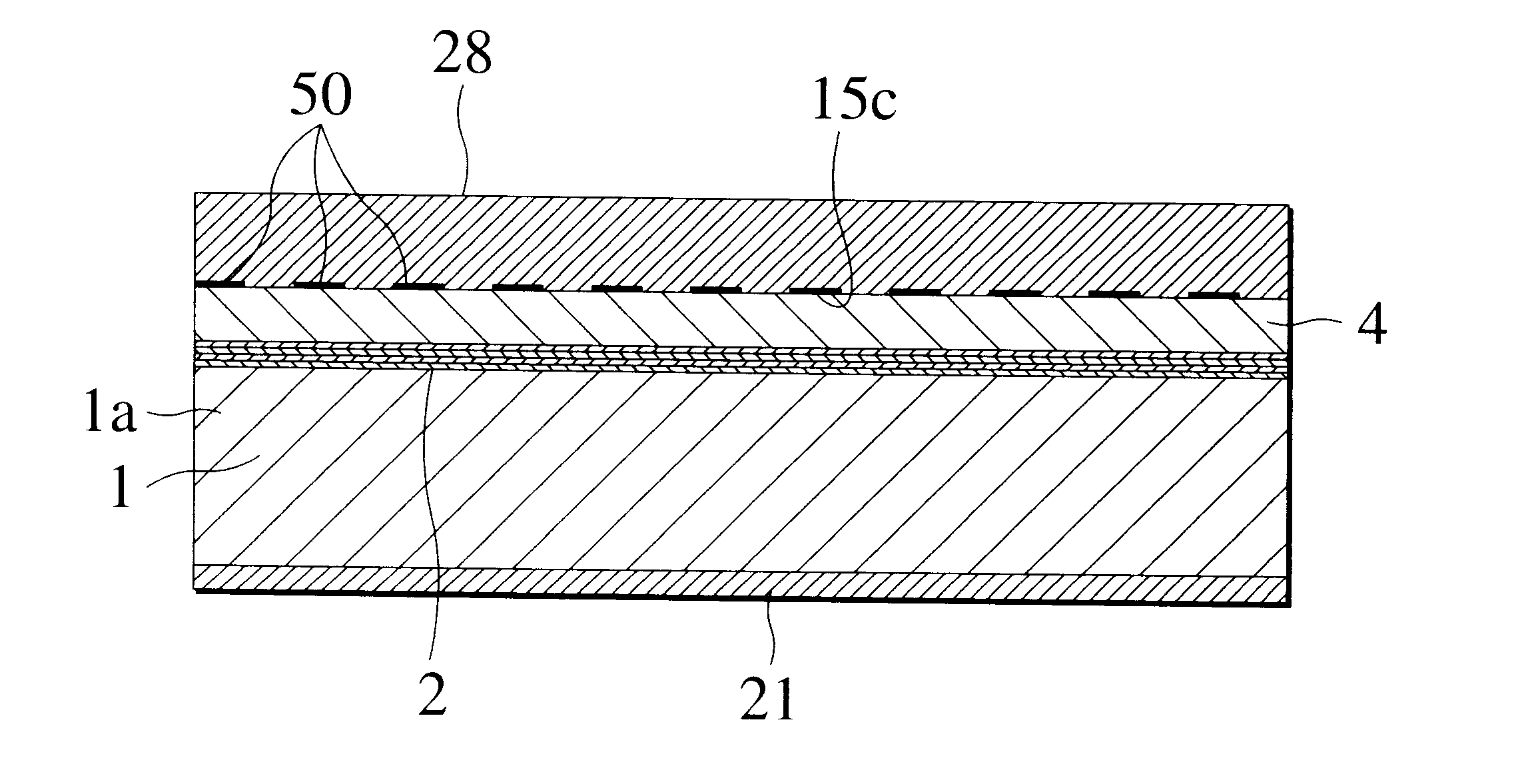
FIG. 9 is a schematic perspective view showing a structure of a laser diode according to a third embodiment of the present invention. The underlying semiconductor layers are formed in the same way as above embodiments. In other words, the MQW active layer 2, the p-InP layer 4, and the p-InGaAsP contact layer 5 are grown on the n-InP substrate 1 (including the n-InP buffer layer 1a). The ITO layer 28 acting as the transparent electrode is stacked and then patterned like a stripe. The refractive index of the ITO layer 28 is adjusted to 3.0.

Then, the ITO layer 29 (preferably 1.5 .mu.m to 2.0 .mu.m in thickness) which has the refractive index (n=2.5) (preferably 2.5 to 2.8) smaller than the refractive index ITO layer 28 is stacked thereon. Then, the ITO layer 29 is patterned like a stripe to bury the ITO laye...


PUM


Abstract

Both an electric energy applying mechanism and an optical waveguide mechanism can be provided to an ITO layer (transparent electrode) by constituting an optical waveguide so as that the guided mode profile spread into the ITO layer. Also a bonding pad is provided to supply a power and apply an electric field onto the ITO layer. Accordingly, a device structure can be simplified and thus improvement in yield of the optoelectronic device having an optical waveguide and improvement in parameters of the optoelectronic device can be achieved.

Description

1. Field of the InventionThe present invention relates to optoelectronic devices which include electrodes and optical waveguides as essential constituent elements and, more particularly, to an electrode structure of laser diodes and their application technology.2. Description of Related ArtThere is a DFB (distributed feedback) laser as one type of laser diodes. This laser diode has a diffraction grating in which a refractive index is changed periodically along the waveguide. The laser diode can oscillate in a single longitudinal mode (SLM) (i.e., one oscillation line) around the Bragg wavelength determined by the period of the diffraction grating. For 6. In this mesa electrode structure, in order to reduce a junction area, the p-side electrode 20 must be formed on the top of a mesa stripe 25 surrounding the active layer and also must be connected to a bonding pad 27 on the thick SiO2 film 26, while taking account of step-recoverage.As described above, in the laser diode in the relat...

Claims


Application Information

Patent Timeline
Patent Type & Authority Patents(United States)
IPC IPC(8): H01S5/00H01S5/187H01S5/042H01S5/12
CPCH01S5/12H01S5/0202H01S5/0425H01S5/1228H01S5/1231H01S5/04253H01S5/2275
Inventor KINOSHITA, JUNICHI
Owner KK TOSHIBA
Why Eureka
Try Eureka