Electrophotographic photoreceptor and its manufacturing method

a photoreceptor and photoreceptor technology, applied in the field of electrostatic photoreceptors, can solve the problems of defect in electrostatic latent image, non-uniform contrast with interference fringe pattern, and interference between incident lights

Inactive Publication Date: 2001-12-18
FUJIFILM BUSINESS INNOVATION CORP
View PDF21 Cites 18 Cited by
  • Summary
  • Abstract
  • Description
  • Claims
  • Application Information

AI Technical Summary

Problems solved by technology

In this case, an interference may be occurred between incident lights being incident on the surface of the photoreceptor from the semiconductor laser and reflected lights produced by reflection of lights on the surface of the conductive support which lights have transmitted through the photoconductive layer on the surface of the photoreceptor.
In particular, when a high gradient is required in a halftone and solid image and an image with horizontal ruled line patterns, there was a problem in which a defect in the electrostatic latent image was apt to occur which might become a cause of the moire fringes when a latent image was formed with a laser.
Its reflected light is believed to make interference with the reflected light from and the incident light onto the surface of the photoconductive layer, resulting in nonuniformity of contrast with the interference fringe pattern.
Further, what causes problems in an electrophotographic photoreceptor is that a local electrification defect based on an imperfection of the photoreceptor, and the defect often causes a conspicuous image failure such as black spots and fogs.
If crystallized particles exist on the conductive support, recesses referred to as pits cause the surface to be uneven, thereby not only affecting manufacture of the photoconductive layer, but also causing an image defective.
These crystallized particles have chemical properties different from that of aluminum, so that they were dissolved antecedently in the anode oxidation treatment to cause the crystallized particles in the neighborhood of the surface to be left out, resulting in generation of pits.
As mentioned above, there were following problems in the prior art.
However, the complete cancellation of the interference fringes can not be achieved because factors of reflected lights still exist.
Further, there were problems such that risk of increasing charge injection from heights made too rough, and also ground fog tends to occur, particularly in white solid printing.
(2) Many rough surface processes conduct the burnishing process or the sand-blasting process as the second processing, after a surface of the conductive support is once subject to the cutting process, so that the productivity was very wrong, therefore, these processes were not suitable for mass production.
In particular, when surface roughness Ry (when a reference length of 0.8 mm is measured in JIS Standard) becomes larger than 2.0 .mu.m, swell and flocculation state on a coating film of the photoconductive layer would be generated, so that not only coating irregularity is apt to be produced, but also stripe like noise becomes a large problem.
On the contrary, when Ry (when a reference length of 0.25 mm is measured in JIS Standard) is less than 0.8 .mu.m, in a case of a photoreceptor, problems such as a light interference and an excessive exposure phenomenon due to a laser would tend to be occurred.
(3) Defectives such as pits or the like can not be prevented even if a high purity aluminum alloy is used for the conductive support.
In addition, a method for decreasing the defectives in the process of the anode oxidation treatment can also not prevent the change of crystallized particles already formed in the course of making an aluminum alloy to be ingot and shaping it to be tubular.
This method uses high purity aluminum alloy and requires a high precision rectifier operation for current, forcing a product to be expensive.
Further, the blocking layer produced using an anodic oxidation film and a macromolecular resin obtained by these methods would be difficult to eliminate an image defective such as black spots and fogs, and in particular, multiple fogs would be generated under the high temperature and humidity environment.
(4) On the other hand, the conventional method using an anodic oxidation film has disadvantages such that variability tends to be generated in the blocking effect and heat-resistant characteristic is poor.
Accordingly, problems would be encountered concerning generation of cracks on the surface during drying process, or coating irregularity, deterioration of electric insulation breakdown strength, or growth of cracks into the photoconductive layer during formation of the photoconductive layer.

Method used


Image

  • Electrophotographic photoreceptor and its manufacturing method
  • Electrophotographic photoreceptor and its manufacturing method
  • Electrophotographic photoreceptor and its manufacturing method

Examples


example

Next, the present invention will be explained in the concrete with reference to embodiments, but is not limited to the following embodiments so long as its spirits are not exceeded.

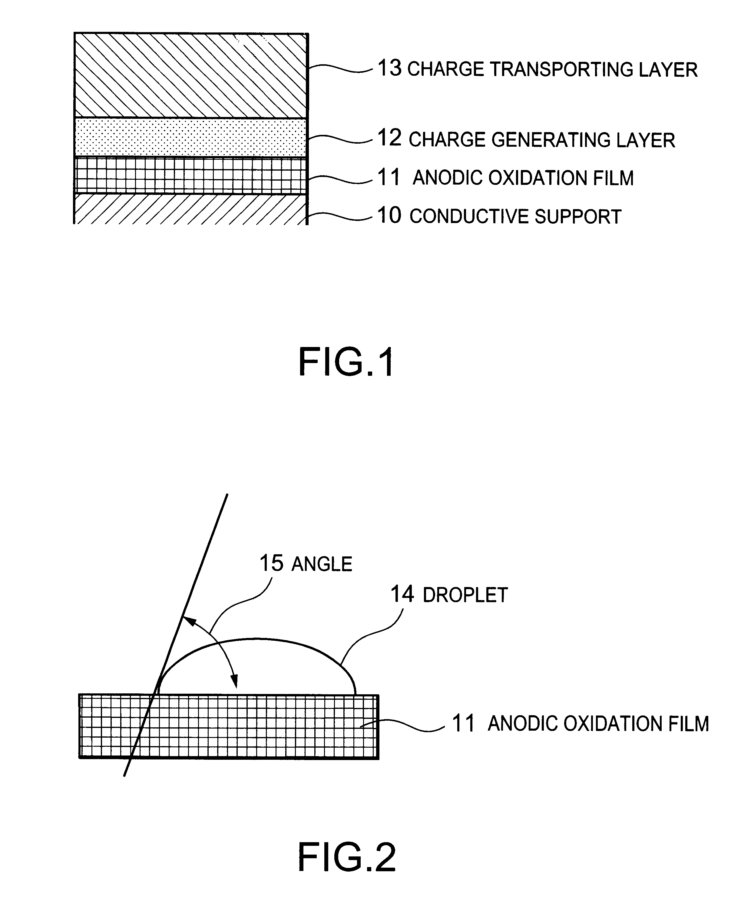
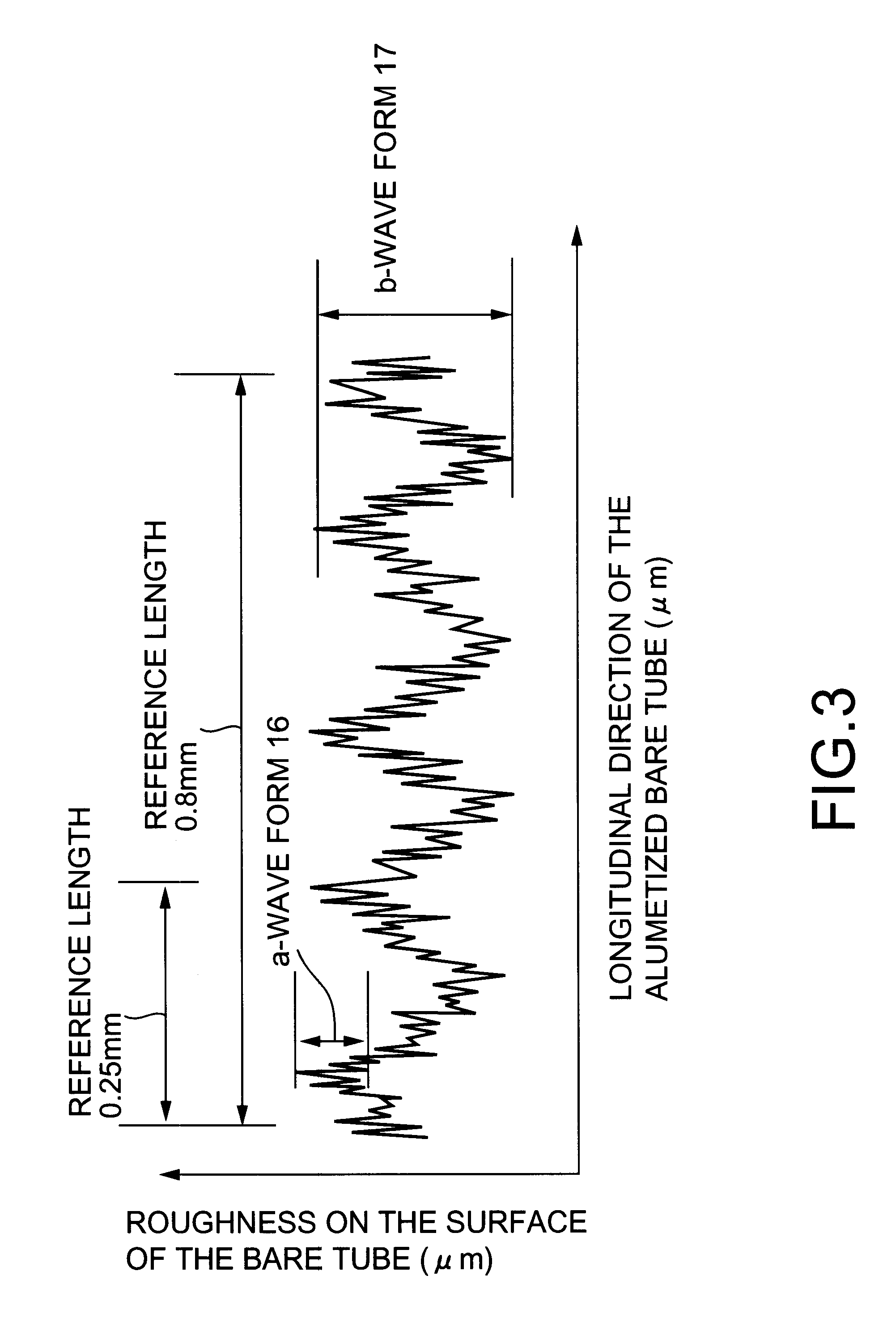
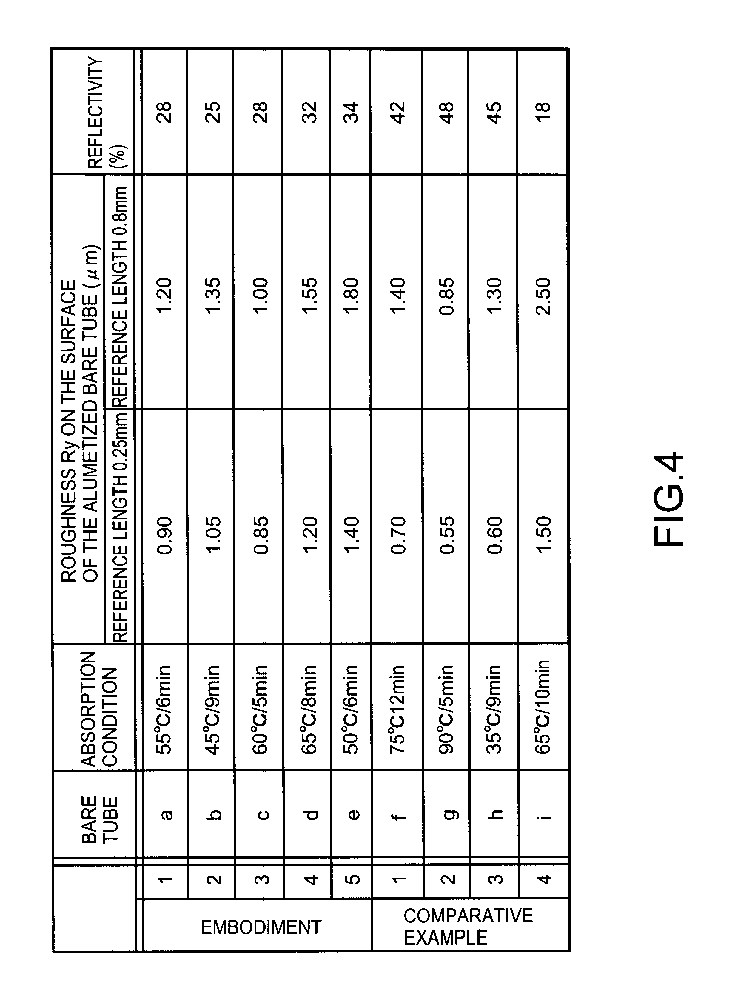
As a material of the conductive support 10, an aluminum alloy of 6000 series in JIS Standard was used, which aluminum alloy was subjected to a hot extrusion process to obtain a cylindrical aluminum bare tube with an external diameter of approximately 30 mm and a length of approximately 350 mm. Using a tool with a blade edge in which sintered diamond chips of a moderate density are adjusted, precise cutting processing for the surface of the bare tube was performed. After the surface cutting has been completed, the bare tube was subjected to degrease and washing process with an organic solvent and followed by etching process, and subsequently, after washed with water, it was subjected to an anode oxidation treatment for 15 minutes using sulfuric acid with a concentration of 150 g / l as an electrolyte solutio...

embodiments 1 to 3

The charge generating layer having a thickness of approximately 0.2 .mu.m was formed by applying a paint to alumetized bare tubes obtained a to c and drying by heating them, which paint was produced by adding 2.5 parts by weight .tau. type metal-free phthalocyanine and 2 parts by weight polyvinyl butyral to 100 parts by weight tetrahydrofuran solution and by dispersing the solution for 24 hours in a ball mill.

Next, after 14 parts by weight 2-methyl-4-dibenzyl amino-benzaldehyde-N,N-diphenyl hydrazone, 6 parts by weight 1,1-bis(palladiethyl aminophenyl)-4,4-diphenyl-1,3-butadiene, and 20 parts by weight polycarbonate (Z-400, which is a product put on the market from Mitsubishi Gas Chemical) were dissolved in 100 parts by weight methylene chloride to immerse and apply on the charge generating layer, the layer was dried by heating to form a charge transporting layer having a thickness of approximately 20 .mu.m, thereby producing the electrophotographic photoreceptors.

embodiments 4 to 5

The charge generating layer having a thickness of approximately 0.15 .mu.m was formed by applying a paint to alumetized bare tubes obtained d to e and drying by heating them, which paint was produced by adding 2 parts by weight titanyl phthalocyanine and 2 parts by weight polyvinyl butyral to 100 parts by weight tetrahydrofuran solution and by dispersing the solution for 24 hours in a ball mill.

Next, after 18 parts by weight .alpha.-phenyl-4-N,N-bis(4-methylphenyl)aminostilbene and 20 parts by weight polycarbonate (Z-400, Mitsubishigasukagaku) were dissolved in 95 parts by weight tetrahydrofuran to immerse and apply on the charge generating layer, the layer was dried by heating to form a charge transporting layer having a thickness of approximately 20 .mu.m, thereby producing the electrophotographic photoreceptors.

The electrophotographic photoreceptors obtained in this way are referred to as drums A to E.


PUM


Abstract

The electrophotographic photoreceptor according to the present invention has a conductive support (10) and a photoconductive layer laminated on the conductive support. The conductive layer is characterized by making a quantity of reflected lights with respect to exposure of a coherent light as a light source to be small and by having a short wavelength surface roughness in order to suppress a quantity of interference lights produced by the reflected lights and reflected lights from or incident lights on the photoconductive layer. Specifically, the conductive support (10) has aluminum or aluminum based alloy, and the maximum height (Ry) of the surface roughness of the conductive support is 0.8 mum or more and 2.0 mum or less. Further, the reflectivity of the light on the surface of the conductive support is equal to or less than 35% of a quantity of exposure light of a light source of a coherent light. This is able to prevent generation of the interference fringes.The surface of the conductive support is preferably processed for an anodic oxidation film. In this case, the surface roughness subjected to the anode oxidation treatment has a roughness waveform composed of two components shown in the following equation: 1.0a<=b<==2.5a, wherein, a is the roughness of the short waveform (fine roughness) component, and b is the roughness of the long waveform (coarse roughness) component.

Description

1. Field of the InventionThe present invention relates generally to an electrophotographic photoreceptor and its manufacturing method utilized particularly in a copying machine, a printer, or a facsimile machine and used when an imaging operation is performed with an electrophotographic process.2. Description of the Related ArtsAs is conventional, an imaging system using an electrophotographic photoreceptor forms a toner image on a surface of the photoreceptor by forming an electrostatic latent image with a laser exposure and by developing the image with toner particles to render the image visible after the surface of the photoreceptor with photoconductive property is charged by the corona discharge. The photoreceptor is composed of a conductive support and a photoconductive layer formed on the conductive support and consists of a charge generating layer and a charge transporting layer. The toner image on the photoreceptor is transferred on a recording medium by a transferring devic...

Claims


Application Information

Patent Timeline
Patent Type & Authority Patents(United States)
IPC IPC(8): G03G5/10G03G5/047G03G5/00G03G5/043
CPCG03G5/00G03G5/047G03G5/10
Inventor MATSUI, NAOYUKI
Owner FUJIFILM BUSINESS INNOVATION CORP
Why Eureka
Try Eureka