Method of manufacturing a semiconductor device using a polymer film pattern

a technology of polymer film and semiconductor, applied in the direction of semiconductor devices, electrical devices, photosensitive material processing, etc., can solve the problems of shrinkage of the volume of water, weakening of the mechanical strength of the silicon substrate, and crystal defects in the silicon substrate, so as to improve the pn junction characteristics and improve the element characteristics markedly

Inactive Publication Date: 2002-10-15
KK TOSHIBA
View PDF8 Cites 85 Cited by
  • Summary
  • Abstract
  • Description
  • Claims
  • Application Information

AI Technical Summary

Benefits of technology

An object of the present invention is to provide a method of manufacturing a semiconductor device, in which a desired ion implantation is applied to a

Problems solved by technology

If ions are implanted into a silicon substrate, crystal defects can be generated in the silicon substrate.
It is commonly known in the art that the crystal defects do not decrease in the subsequent heat treatment, thus causing the weakening of the mechanical strength of the silicon substrate by multiple repetitions of the ion implantation and the heat treatment process.
It is commonly understood that one of the causes of a crack may be attributable to the fact that water within the photoresist was initially frozen then when submitted to heat treatment, the volume of the water expands.
If cracks are generated in the resist, ions are implanted into the masked region, too, so as to deteriorate the pn junction characteristics, resulting in failure to obtain a desired atomic characteristic.
In the worst scenario, cracks can also be generated in the underlying insulating film where the cracks are generated on the resist pattern.
The problem is that, if a crack is generated in the photoresist, ions are implanted into an undesired region.
As a result, the leak current through the pn junction is increased by at least two folds and, thus, it may not be possible to obtain good element characteristics.
However, an additional problem is generated in the case of using a dummy gate.
Specifically, a damascene gate MOSFET is a transistor of high performance as compared to a MOSFET, but requires a long manufacturing process.
Since the width of the dummy gate is determined in view of the irregularity noted above, the processing accuracy of the gate size is poor.
Incidentally, even if an amorphou

Method used


Image

  • Method of manufacturing a semiconductor device using a polymer film pattern
  • Method of manufacturing a semiconductor device using a polymer film pattern
  • Method of manufacturing a semiconductor device using a polymer film pattern

Examples


example i

FIG. 7 shows a cross sectional view of a schematic drawing of the construction of a CMOS-FET 10 in performing an ion implantation in a method according to an embodiment of the present invention.

CMOS-FET 10 may be prepared as follows. First, an n-type well 12, a p-type well 13, and an element isolating insulating film 14 are formed on a semiconductor substrate 11. Second, after formation of a gate insulating film 15 on semiconductor substrate 11, a gate electrode or a dummy gate 16 is formed, followed by implanting ions of B or BF.sub.2 into semiconductor substrate 11 in a concentration of approximately 1.times.10.sup.14 to 5.times.10.sup.15 cm.sup.-2 so as to form a p-type impurity layer 17.

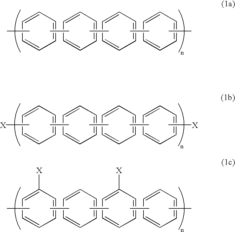
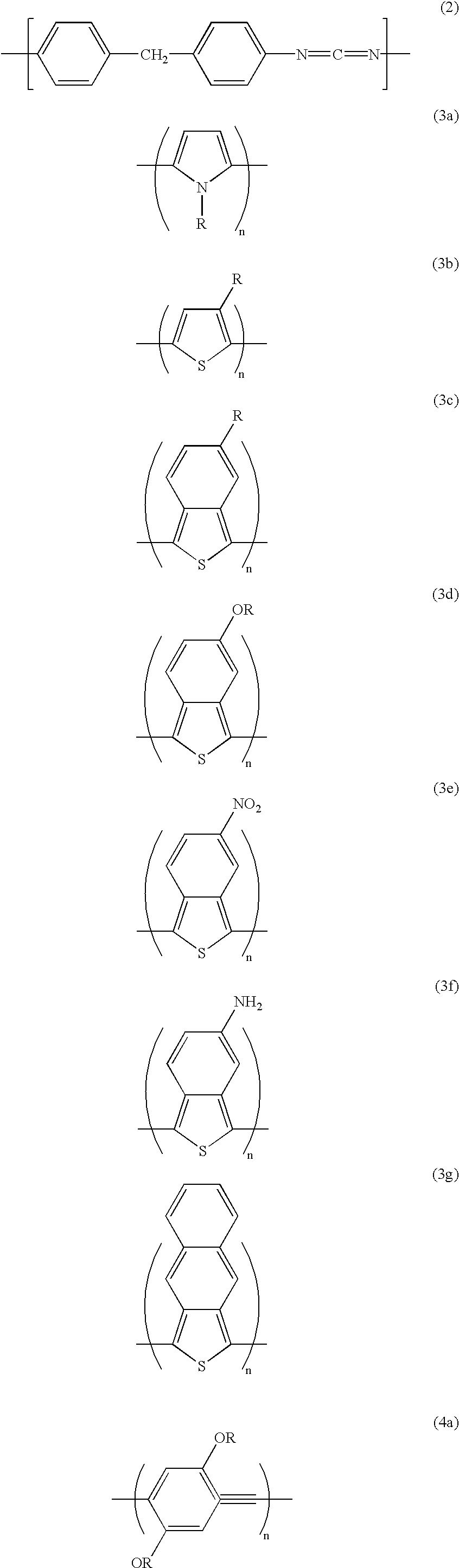
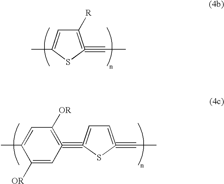
A mask 18 for implanting ions of an n-type impurity 19 may be prepared by using a polymer having a carbon content higher than a hydrogen content. The polymer used in accordance with the present invention may include, for example, a polymer containing about 60% of carbon by atomic ratio, about 1 t...

example ii-1

Manufacturing Method of a Damascene Gate MOSFET Using a Polymer as a Damascene Gate

In the manufacturing process of a transistor, it is important to carry out heat treatment in order to activate implanted ions. Therefore, the following experiment was conducted in order to confirm whether or not the polymer is capable of withstanding the heat treatment.

FIG. 8 is a graph showing experimental data with respect to the heat resistance of a polymer film. Specifically, the experiment was conducted by applying heat to a polymer film, while changing the atomic ratio of carbon to hydrogen of the polymer film. The heat was applied for one hour to simulate a heat treatment during a manufacturing process, and the heat resistance of the polymer film was evaluated in terms of the "applicable temperature" which does not bring about deformation of the film by thermal decomposition (degassing), peeling of the film, or cracking. In addition to carbon and hydrogen, oxygen is also present in the polymer ...

example ii-2

FIGS. 12 to 14 collectively show a method of manufacturing a transistor according to another embodiment of the present invention. Like reference numerals are used to denote elements similar to those in Example II-1 previously described. Example II-2 differs from Example II-1 in that Example II-2 comprises the step of increasing the thickness of the oxide film in extension region 35 of the source-drain region on the surface of semiconductor substrate 31, after the formation of dummy gate 34.

First, structure 30" shown in FIG. 12 is prepared. Specifically, a groove is formed by dry etching on the surface of silicon semiconductor substrate 31, followed by forming insulating film 32 within the groove by means of deposition or coating for element isolation. Similarly, a silicon oxide film can be used as insulating film 32. Alternatively, a silicon nitroxide ("SiNO") film with a thermal expansion coefficient close to that of silicon, i.e., about 3 ppm / K can also be used. The surface of ins...


PUM


Abstract

Claimed and disclosed is a method of manufacturing a semiconductor device, the method comprising the steps of forming a dummy gate on a semiconductor substrate, forming a source-drain diffusion region by introducing an impurity into the semiconductor substrate having the dummy gate as a mask, removing the dummy gate to form an opening, and forming a gate electrode within the opening with a gate insulating film formed below the gate electrode. The dummy gate is further formed by coating the semiconductor substrate with a polymer having a higher carbon content than hydrogen content so as to form a polymer film, forming a photoresist pattern on the polymer film, and transferring the pattern shape of the photoresist pattern onto the polymer film.

Description

1. Field of the InventionThe present invention directs to a method of manufacturing a semiconductor device, particularly, to a method of manufacturing a semiconductor device featured in the ion implantation step and to a method of manufacturing a semiconductor device featured in the step of forming the gate electrode of a transistor.2. Description of the Related ArtIn recent years, a large scale integration ("LSI"), in which many transistors and resistors are connected to each other to form an electric circuit and are mounted integrally on a single chip, could be used in some portions of an electronic computer or a communication appliance. Therefore, the performance of an entire apparatus can be heavily related to the performance of the LSI single body. The performance of the LSI single body can be improved by increasing the degree of integration, i.e., by improving the elements quality of the chips.The elements can be improved by rendering optimum the ion implantation for forming t...

Claims


Application Information

Patent Timeline
IPC IPC(8): H01L21/336H01L21/02G03F7/40H01L21/027H01L21/265H01L21/28H01L21/8238H01L21/8242H01L27/092H01L27/108H01L29/423H01L29/43H01L29/49H01L29/78
CPCH01L29/66545H01L29/6659H01L29/66537H01L21/265
Inventor SUGURO, KYOICHIMATSUO, KOUJIMURAKOSHI, ATSUSHISATO, YASUHIKONIIYAMA, HIROMI
Owner KK TOSHIBA
Why Eureka
Try Eureka