Method of producing a single crystal gallium nitride substrate and single crystal gallium nitride substrate

a gallium nitride and substrate technology, applied in the direction of crystal growth process, monocrystalline material growth, semiconductor lasers, etc., can solve the problems of gan/sapphire lds to other difficulties, gan/sapphire lds to incur an extra cost,

Inactive Publication Date: 2002-10-22
SUMITOMO ELECTRIC IND LTD
View PDF9 Cites 204 Cited by
  • Summary
  • Abstract
  • Description
  • Claims
  • Application Information

AI Technical Summary

Benefits of technology

The basic idea is simple. But there are many sets of assemblies of the growing surfaces and the slicing surfaces which can realize this invention, because many crystallographic planes exist in a GaN single crystal. An increase of the times of growth enhances the number of available sets.

Problems solved by technology

Lack of natural cleavage compels device makers to cut (dice) mechanically sapphire wafers crosswise and lengthwise into device chips with an application of strong forces.
The dicing process incurs an extra cost and decreases a yield in the production of GaN LEDs.
Uncleavability of GaN crystals subjects GaN / sapphire LDs to other difficulties besides the problems of dicing.
Uncleavable GaN prevents GaN laser diodes from making resonator mirrors by natural cleavage, which invites difficulties on laser oscillation performance and on production cost.
Another difficulty originates from the fact that sapphire is an insulator.
The extra etching, the extra thick film and an extra wirebonding raise the cost by increasing the time of fabrication and the number of steps.
This point incurs an increment of the cost.
The sapphire substrates are suffering from these difficulties.
Silicon carbide, however, has some drawbacks.
Single crystal silicon carbide is highly expensive.
The difficulty of producing SiC single crystals will jeopardize a continual, stable supply of SiC substrates.
The crystalline property of GaN films grown on SiC substrates are still bad at present.
SiC is not deemed to be the suitable material as a substrate of GaN light emission devices.
GaN / SiC LEDs are not brought onto market yet.
Sapphire or silicon carbide as a substrate induces many dislocations and other defects in GaN type films grown thereupon owing to mismatches of lattice constants and thermal expansion coefficients between the upper films and the bottom substrate.
However, in the case of GaN / sapphire LDs which require large current density, experiments clarify the fact that the big dislocation density forbids the on-sapphire GaN type LDs from having a long lifetime.
The big current increases the dislocations and other defects.
The fabrication of the resonator mirror would raise the cost of GaN / sapphire LDs.
The high cost and short lifetime degrade sapphire as a substrate for GaN LDs.
From the reasons, sapphire and silicon carbide are not the most suitable material for the substrates of GaN LDs.
However, crystal growth technology has not been matured for GaN yet.
It is difficult at present to produce gallium nitride single crystals with a large size sufficient for the substrates of GaN LDs.
However, even if it succeeded, the ultrahigh pressure method would synthesize only a small GaN crystal which would be insufficient for the substrate of GaN LDs.
Such a liquid phase method is hopeless for supplying wide gallium nitride crystals on an industrial scale.
It is impossible to eliminate the sapphire substrate from the GaN film, since there is no means of removing the hard, sturdy sapphire.
Some defects accompany the GaN wafers produced by the method of FIG. 5.
The most serious problem is residuals of threading dislocations on the top surface.
The rapid degeneration would raise the threshold current and would curtail the lifetime.
The ELO-made GaN wafers are not suitable for LDs yet.
If there is no mechanism of killing dislocations, low dislocation density crystal cannot be obtained.
It is rather difficult to identify the crystal orientations.
This method, however, is subject to accumulation of dislocations at the bottoms of the facet-pits.
The localized accumulation of dislocations decreases the device properties and the yield.
The LDs fabricated upon the dislocation accumulated regions would be rejected at the inspection, which would decrease the yield.
The accumulated dislocations impede the GaN from cleaving by disturbing the regularity of lattices.
Another problem of the GaN crystal having highly accumulated dislocations is disorder of cleavage.
The extra step of polishing would raise the manufacturing cost.
High rigidity would require a long time for polishing.
Highly expensive GaN would be overwhelmed by inexpensive, accustomed sapphire.
The prior substrate is suffering from plenty of dislocations.
But if two conditions are equivalent, elimination of one is undesirable.
On the contrary, the extensions of threading dislocations are not easily confirmed.
The definition through the dislocation extensions incurs a difficulty of determining dislocation extensions.
Some directions are more suitable but other directions are less suitable for growing single crystals in their directions.
Few C-plane GaN single crystals have been made due to immature technology.
However, there is neither A-substrate nor M-substrate of a practical size.
Many probable sets of successive growing directions increase the difficulty of intuitive understanding.
This "Cc;C" which would be the most popularly-thought prior art has not been realized in practice due to the lack of a wide C-GaN substrate yet.
The modes "a;A" and "m;M" are still unrealistic.
Since the number of claims is large, it is not easy to understand the mutual relations among the claims.

Method used


Image

  • Method of producing a single crystal gallium nitride substrate and single crystal gallium nitride substrate
  • Method of producing a single crystal gallium nitride substrate and single crystal gallium nitride substrate
  • Method of producing a single crystal gallium nitride substrate and single crystal gallium nitride substrate

Examples


embodiment 1-c

(EMBODIMENT 1-c) Formation of Windows on the SiO.sub.2 Mask

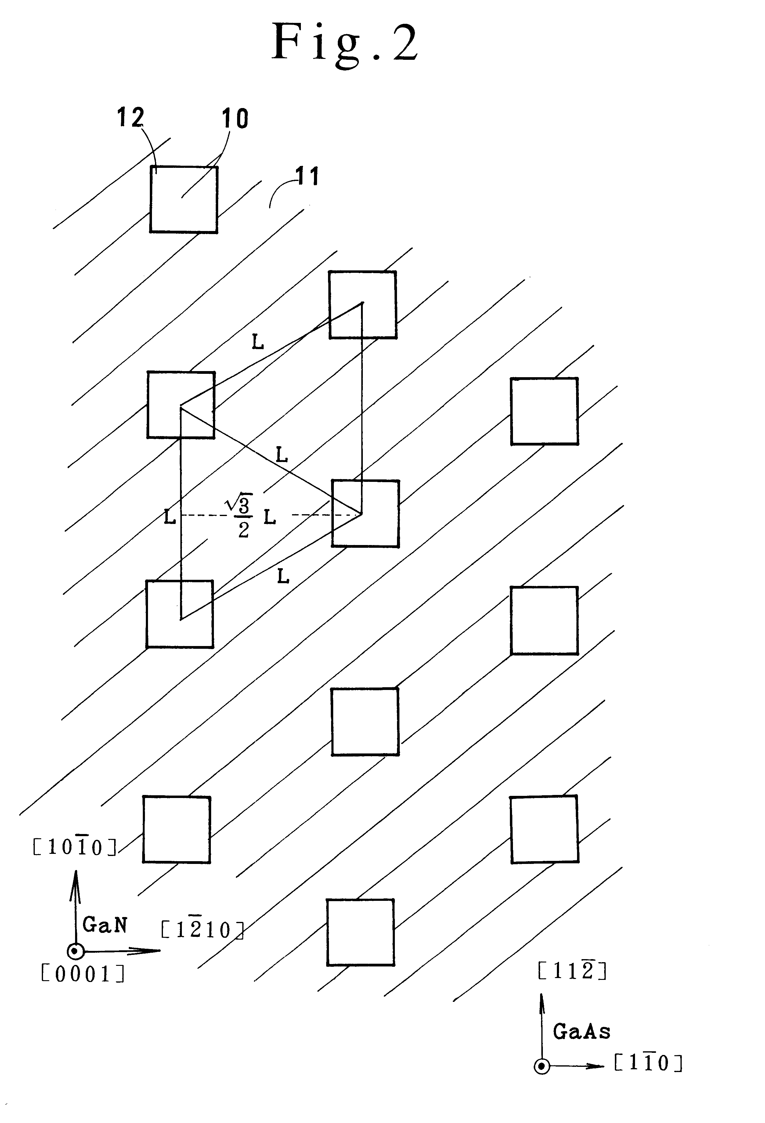
Stripe-shaped, dot-shaped or other shaped windows are available. Here, dot-shaped windows are perforated on the mask. The disposition of the windows is the same as FIG. 2. The square windows are replaced by round dots. The dot has a diameter of about 2 .mu.m. As shown in FIG. 2, a series of windows are regularly aligned along a line extending in a GaAs direction by a 4 .mu.m pitch. Another series of windows are also regularly aligned along another line parallel with and being distanced from the former line by 3.5 .mu.m with half pitch off-set. The window pattern on the pairing lines are repeated in the GaAs [1-10] direction which is orthogonal to the GaAs direction. Namely all the series of windows deviate by 2 .mu.m in the GaAs direction from the neighboring series. Every neighboring three windows are laid on comers of an equilateral triangle of 4 .mu.m sides.

embodiment 1-d

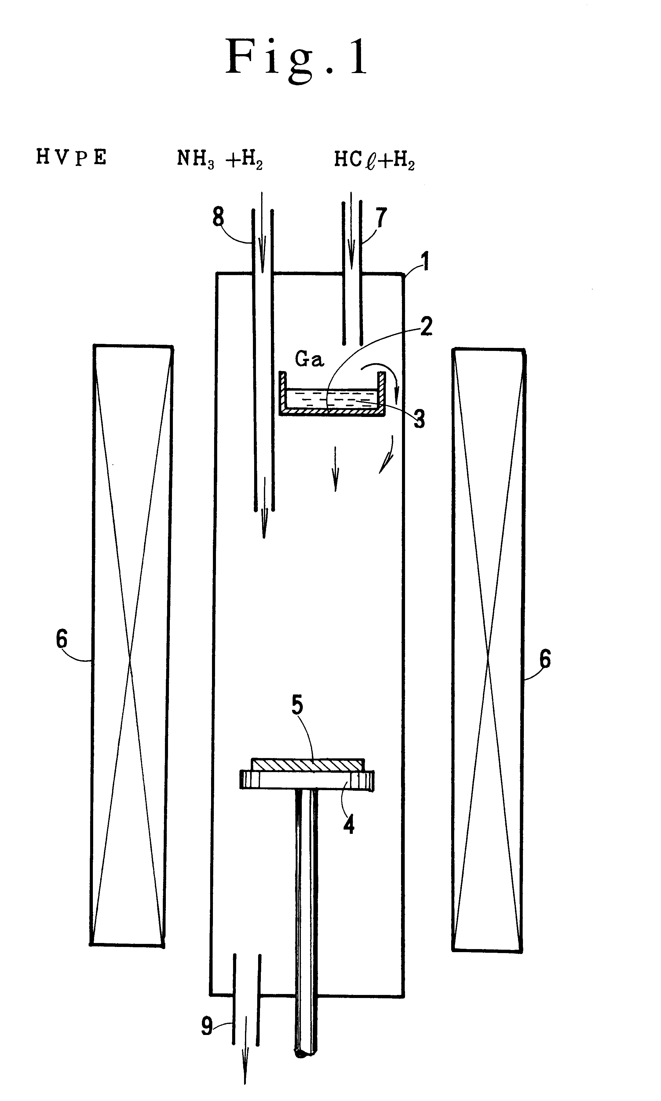
(EMBODIMENT 1-d) HVPE Apparatus

The GaAs substrate with the window-carrying mask is laid upon the susceptor 4 in the furnace 1 of the HVPE apparatus as shown in FIG. 1. The HVPE apparatus is designed to be suitable for a long time growth. A GaN freestanding substrate requires a long time growth of GaN.

The Ga-boat 2 and the susceptor 4 are heated by the heater 6. The Ga is molten in the Ga-boat 2. A mixture of H.sub.2 and HCl gas is supplied to the Ga-melt 3 through the gas inlet 7. Another mixture of H.sub.2 and NH.sub.3 gas is replenished to a space above the susceptor 4 in the furnace 1.

HCl gas with a carrier H.sub.2 gas is supplied to the Ga-melt heated at about 800.degree. C. Reaction of HCl with Ga makes gallium chloride (GaCl) vapor. The GaCl vapor flows downward near the heated GaAs substrate 5 and reacts with ammonia gas NH.sub.3. The reaction synthesizes GaN. GaN molecules are piled upon the heated GaAs substrate 5. Piling of the GaN makes GaN isolated thin films in the wind...

embodiment 1-e

(EMBODIMENT 1-e) Formation of GaN Buffer Layers

The HVPE apparatus makes about 80 nm thick buffer layers upon the revealed surface of the GaAs substrate within the windows under the condition,

The mask SiO.sub.2 has a function of rejecting piling of GaN. No GaN film is deposited on the mask. Since the buffer layers (80 nm) are thinner than the thickness (100 nm) of the mask, the buffer layers are enclosed by the window walls and are separated from other buffer layers by the mask material. The buffer layers which are synthesized at a low temperature (500.degree. C.) play the role of alleviating the misfit of the lattice constants between GaN and GaAs.


PUM

PropertyMeasurementUnit
thicknessaaaaaaaaaa
heightaaaaaaaaaa
heightaaaaaaaaaa

Abstract

GaN single crystal substrates are produced by slicing a GaN single crystal ingot in the planes parallel to the growing direction. Penetration dislocations which have been generated in the growing direction extend mainly in the bulk of the GaN substrate. A few of the threading dislocations appear on the surface of the GaN substrate. GaN substrates of low-dislocation density are obtained.

Description

1. Field of the InventionThis invention relates to a method of producing a single crystal gallium nitride (GaN) substrate and a gallium nitride substrate itself for making light emitting devices of light emitting diodes (LEDs) or laser diodes (LDs) built with the nitride semiconductors consisting of the group 3-5 elements. Gallium nitride and the like (GaInN, AlInN, InAlGaN) are semiconductors having wide band gaps which correspond to blue light or blue / green light.This application claims the priority of Japanese Patent Application No. 2000-207783 filed on Jul. 10, 2000 which is incorporated herein by refernce.2. Description of Related ArtBlue-light LEDs making use of the nitride semiconductor (GaN, GaInN, AlInN, AlInGaN) have been already put into practice on mass scale. There is no natural single crystal GaN mineral. It has been impossible to grow gallium nitride (GaN) single crystal ingots from a GaN melt, since heating converts solid phase GaN directly into vapor phase GaN witho...

Claims


Application Information

Patent Timeline
Patent Type & Authority Patents(United States)
IPC IPC(8): C30B25/02H01L21/20H01L21/02H01L21/301C30B29/38H01L33/32H01S5/323
CPCC30B25/02C30B29/406H01L21/02389H01L21/02395H01L21/0242H01L21/02433H01L21/02458H01L21/0254H01L21/02546H01L21/20
Inventor MOTOKI, KENSAKUKASAI, HITOSHIOKAHISA, TAKUJI
Owner SUMITOMO ELECTRIC IND LTD
Why Eureka
Try Eureka