

Method of manufacturing GaN ingots
a manufacturing method and technology of ingots, applied in the direction of aftertreatment details, condensed vapors, under protective fluids, etc., can solve the problems of reducing the performance of gan-based devices, high defect density in device structures, and lack of gan and aln substrates
- Summary
- Abstract
- Description
- Claims
- Application Information
AI Technical Summary
Benefits of technology
Problems solved by technology
Method used
Image

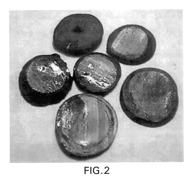
Examples
embodiment 2
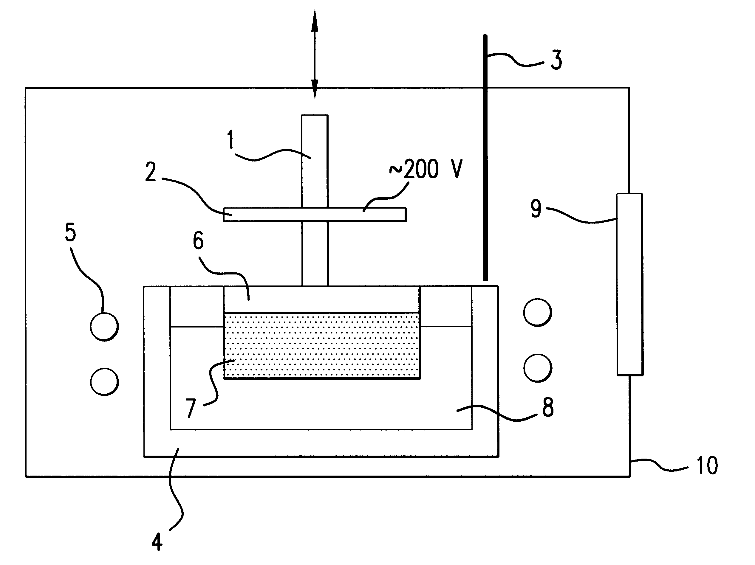
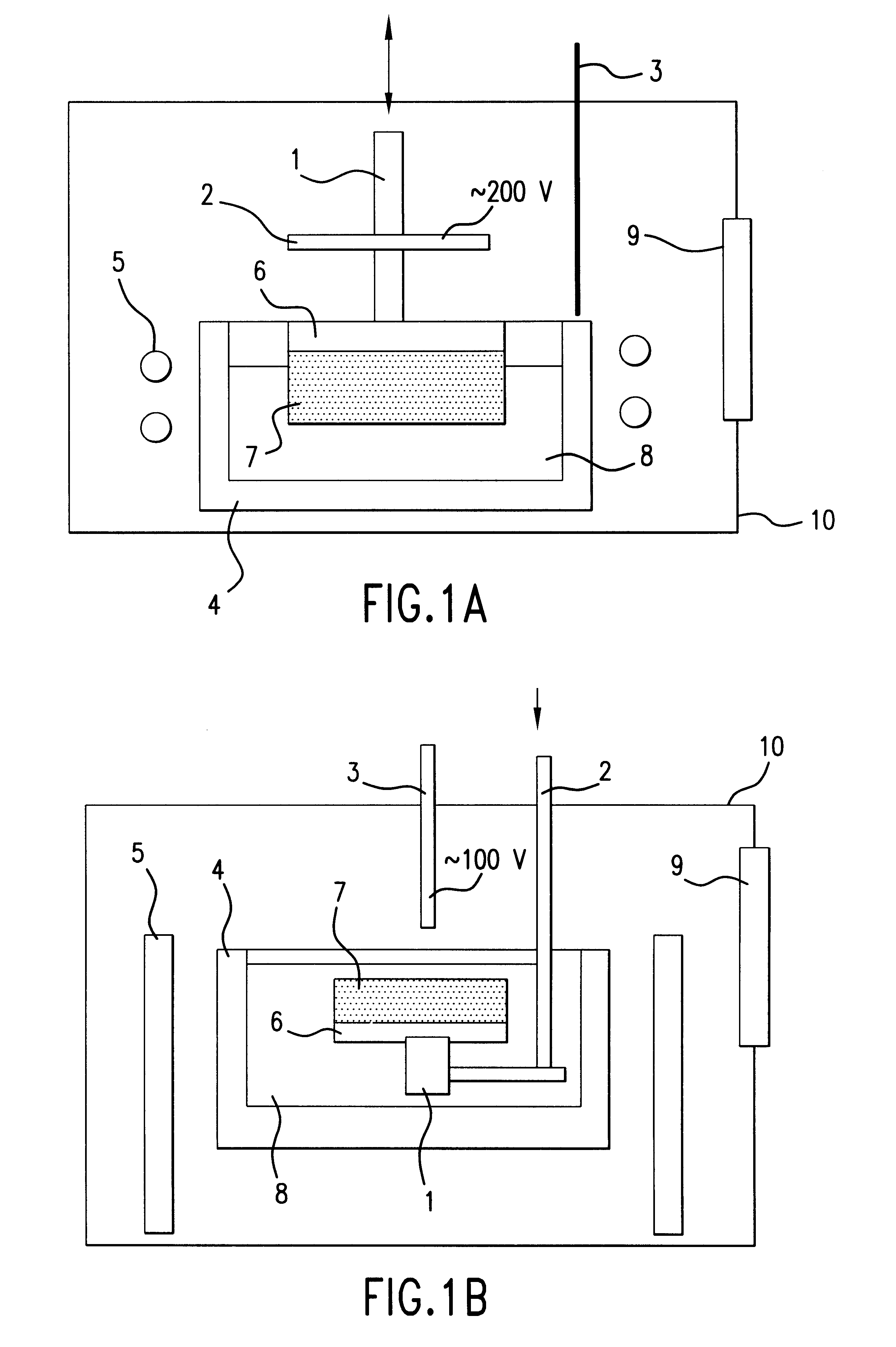
In another experiment, In--Ga alloy was used as a melt for GaN growth. Ga concentration in the melt was 20 at. %. Reactor chamber, where the process took place, was filled with nitrogen gas. Gas pressure was 0.5 atm. Pulsed electric field was applied to grow GaN ingots. The maximum strength of the field was of about 200 V / cm at the melt surface. SiC substrate 35 mm in diameter was used as a seed. GaN was deposited on (0001)Si face of 6H--SiC seed. SiC seed was introduced into the melt. Melt temperature was 1000.degree. C. at the beginning of the growth. During the growth, the melt was cooled down to 900.degree. C. As a result of the growth, GaN ingot 40 mm in diameter and 10 mm long was grown.
embodiment 3
The growth of RP bulk GaN was performed in gallium-bismuth meltsolution placed in a rf-heated graphite crucible. Ga concentration in the melt was 80 at. %. A pressure of nitrogen-hydrogen ambient atmosphere was kept at 0.1 atm. The temperature of the melt was 800.degree. C. GaN crystal was nucleated on GaN single crystal seed. This seed was fabricated in a separate growth run by hydride vapor phase epitaxy. Electric AC field was applied in between two electrodes situated close to the melt surface. Ga covered the surface of GaN ingot, which was pushed inside the melt during the growth. The pushing rate varied from 0.01 to 3 mm / hr. In this case, GaN was grown close to the melt-solution surface. Crucible was rotated. Temperature gradient exists in the melt-solution. Temperature of the melt surface is higher than the temperature in the melt volume. At the end of the growth run, the rf power and electric field was switched off and the melt was rapidly cooled down. Grown crystals were rem...
embodiment 4
The GaN bulk crystal having 50 mm in diameter was grown from the liquid phase at reduced ambient pressure in accordance with the following steps:
(1) The 40 g of as pure as 99.99999% Ga was loaded in a graphite crucible.
(2) The crucible was placed in 90 mm diameter and 110 mm height resistive heater connected to 5 kW power supply.
(3) The stainless steel reactor was totally exhausted by a vacuum pump, hydrogen was introduced into the reactor, thus replacing the air in the reactor with hydrogen gas.
(4) Thereafter, the crucible was heated up to 700.degree. C. by the heater, and this state was held for 30 min to remove the oxide film from the surface of the melt.
(5) The temperature of the heater was decreased down to room temperature and reactor was secondly pumped out down to 10.sup.-3 Torr.
(6) Subsequently, pure nitrogen gas was supplied from the injection pipe to fill the reactor up to 20 Torr gas pressure.
(7) Thereafter, temperature of the resistive heater was increased to 980.degree...
PUM
 Abstract
Description
Claims
Application Information