

Copper-clad board suitable for making hole with carbon dioxide laser, method of making hole in said copper-clad board and printed wiring board comprising said copper-clad board
a carbon dioxide laser and copper-clad board technology, which is applied in the direction of dielectric characteristics, printed element electric connection formation, light absorption dielectrics, etc., can solve the problems of low processing speed, difficult to form fine patterns, and inability to produce high-density printed wiring boards, etc., to facilitate the absorption of carbon dioxide gas lasers and processing rates remarkable highs
- Summary
- Abstract
- Description
- Claims
- Application Information
AI Technical Summary
Benefits of technology
Problems solved by technology
Method used
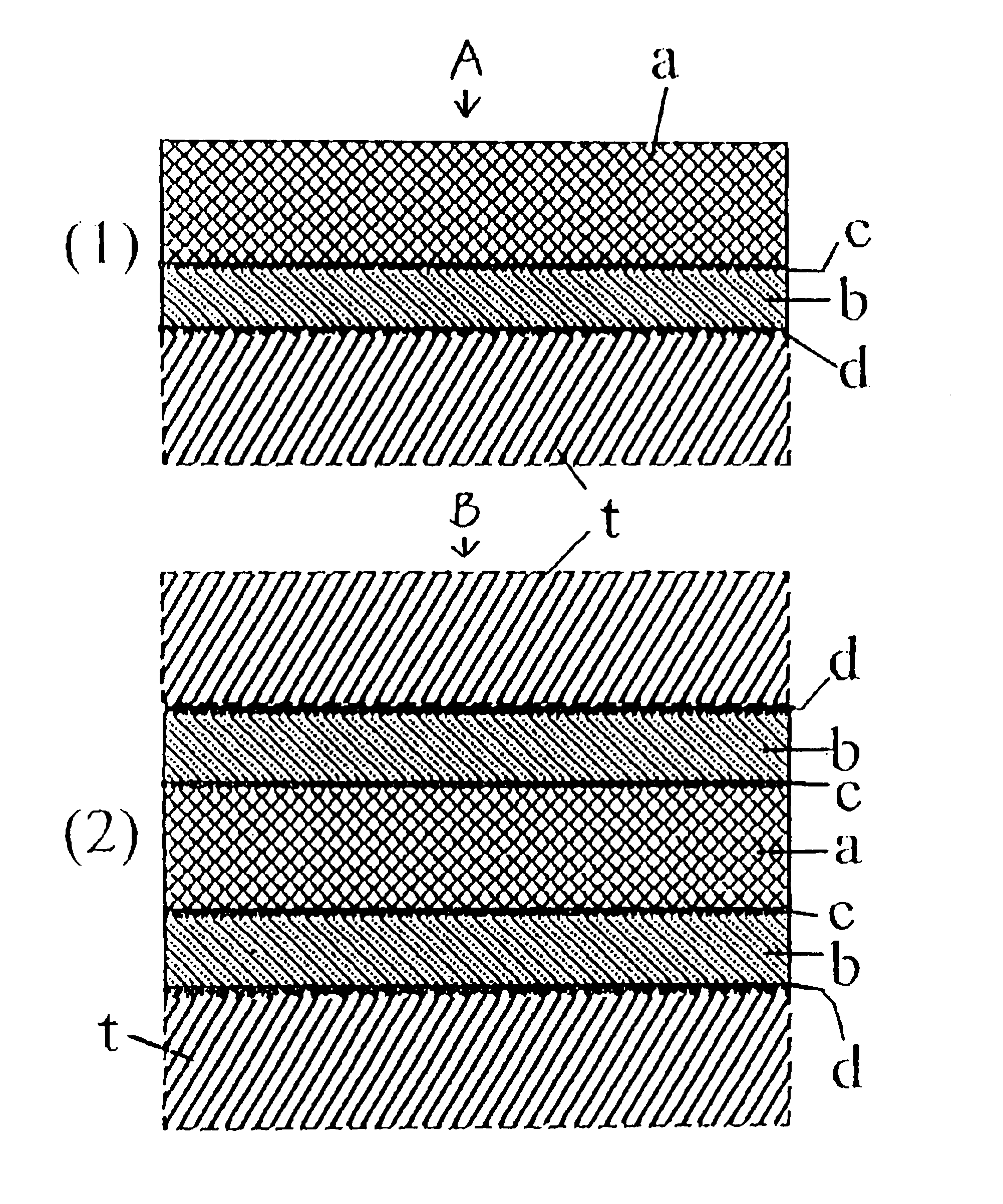
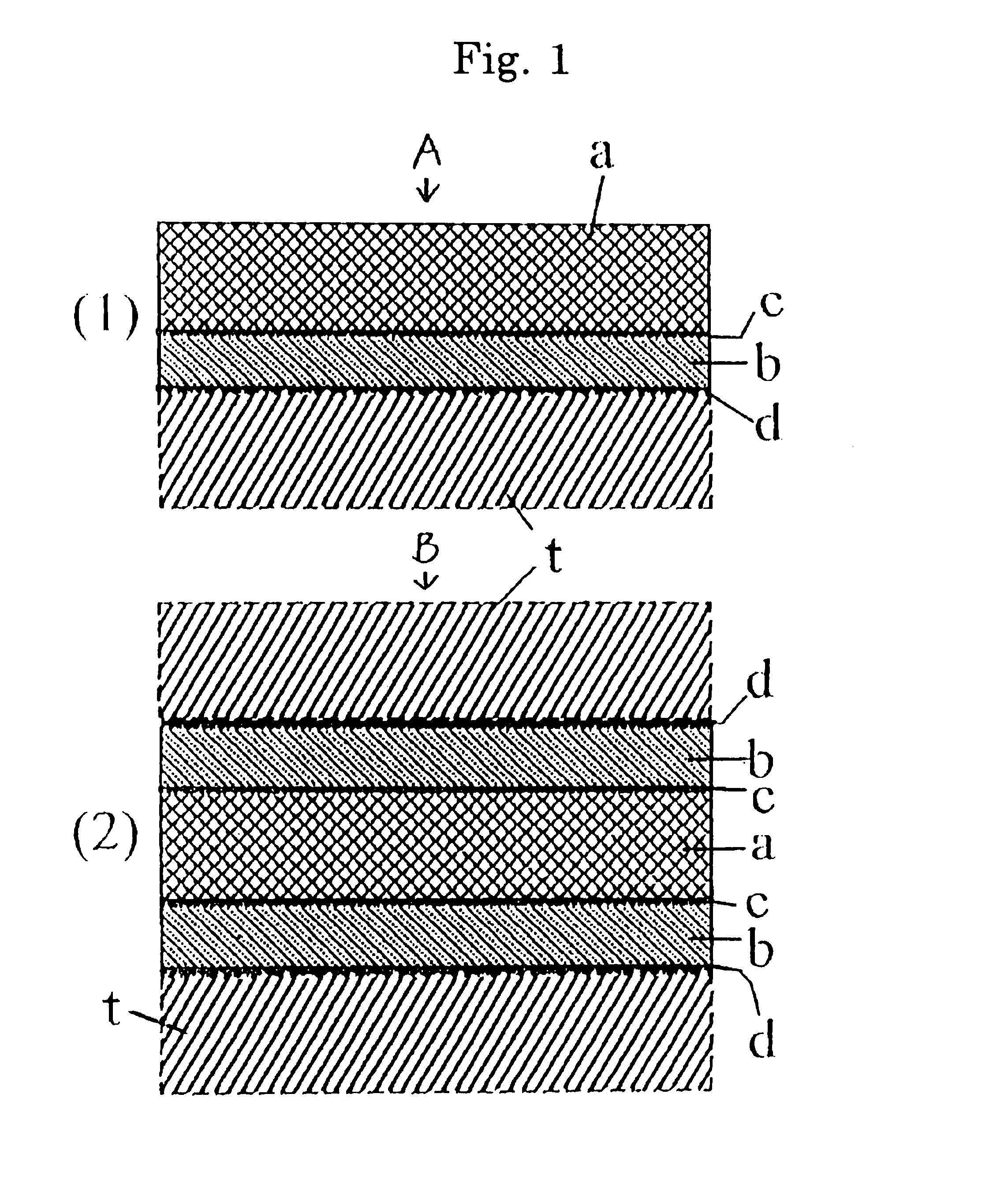
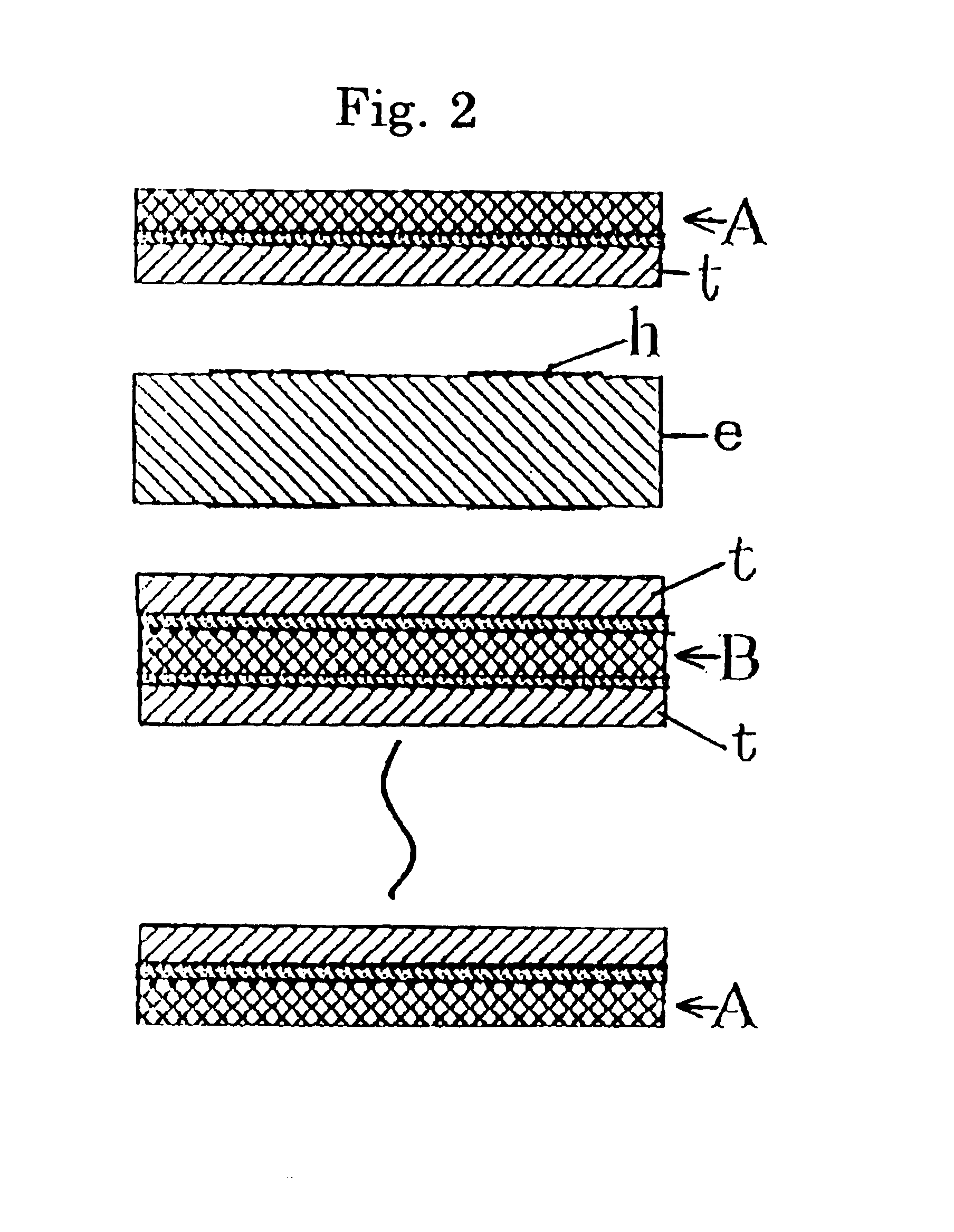
Image

Examples
example 1
700 Parts of 2,2-bis(4-cyanatophenyl)propane, 200 parts of 1,4-dicyanatebenzene and 100 parts of bis(4-maleimidephenyl)methane were melted at 150.degree. C. and allowed to react for 5 hours with stirring, to prepare a prepolymer. The prepolymer was dissolved in mixed solvents of methyl ethyl ketone and dimethylformamide. To this solution were added 400 parts of a bisphenol A type epoxy resin (trade name: Epikote 1001, supplied by Yuka-Shell Epoxy K.K.) and 600 parts of a cresol novolak type epoxy resin (trade name: ESCN-220F, supplied by Sumitomo Chemical Co., Ltd.), and these materials were homogeneously dissolved and mixed. Further, as a catalyst, 0.4 part of zinc octylate was added, and these materials were dissolved and mixed. To the resultant mixture were added 1,000 parts of an inorganic filler (trade name: Calcined Talc, average particle diameter 4 .mu.m, supplied by Nippon Talc K.K.), 1,000 parts of aluminum hydroxide (average diameter 3 .mu.m) and 8 parts of a black pigment...
example 2
300 Parts of an epoxy resin (trade name; Epikote 1001, supplied by Yuka-Shell Epoxy K.K.) and 700 parts of an epoxy resin (trade name: ESCN-220F, supplied by Sumitomo Chemical Co., Ltd.), 35 parts of dicyandiamide and 1 part of 2-ethyl-4-methylimidazole were dissolved in mixed solvents of methyl ethyl ketone and dimethylformamide, and these materials were uniformly stirred and mixed, to give a varnish. The varnish was used to impregnate a 100 .mu.m thick glass woven fabric and dried to give prepreg A having a gelation time of 150 seconds and having a glass fabric content of 48% by weight, and the varnish was used to impregnate a 50 .mu.m thick glass woven fabric and dried to give prepregs B having a gelation time of 170 seconds and having a glass fabric content of 31% by weight.
One sheet of the prepreg A was provided, general electrolytic copper foils having a thickness of 12 .mu.m each were placed on the front and reverse surfaces of the prepreg A, one on one surface and one on the...
example 3
900 Parts of 2,2-bis(4-cyanatophenyl)propane and 100 parts of bis(4-maleimidophenyl)methane were melted at 150.degree. C. and allowed to react for 4 hours with stirring, to prepare a prepolymer. The prepolymer was dissolved in mixed solvents of methyl ethyl ketone and dimethylformamide. To this solution were added 400 parts of a bisphenol A type epoxy resin (trade name: Epikote 1001, supplied by Yuka-Shell Epoxy K.K.), 600 parts of a cresol novolak type epoxy resin (trade name: ESCN-220F, supplied by Sumitomo Chemical Co., Ltd.) and 500 parts of a phenol novolak type epoxy resin (trade name: DEN439, supplied by Dow Chemical), and these materials were homogeneously dissolved and mixed. Further, as a catalyst, 0.4 part of zinc octylate was added, and these materials were dissolved and mixed. To the resultant mixture were added 2,000 parts of an inorganic filler (trade name: Calcined Talc, supplied by Nippon Talc K.K., average particle diameter 4 .mu.m) and 8 parts of a black pigment, ...
PUM
| Property | Measurement | Unit |
|---|---|---|
| energy | aaaaa | aaaaa |
| diameter | aaaaa | aaaaa |
| energy | aaaaa | aaaaa |
Abstract
Description
Claims
Application Information