

Self-assembled photonic crystals and methods for manufacturing same
- Summary
- Abstract
- Description
- Claims
- Application Information
AI Technical Summary
Benefits of technology
Problems solved by technology
Method used
Image

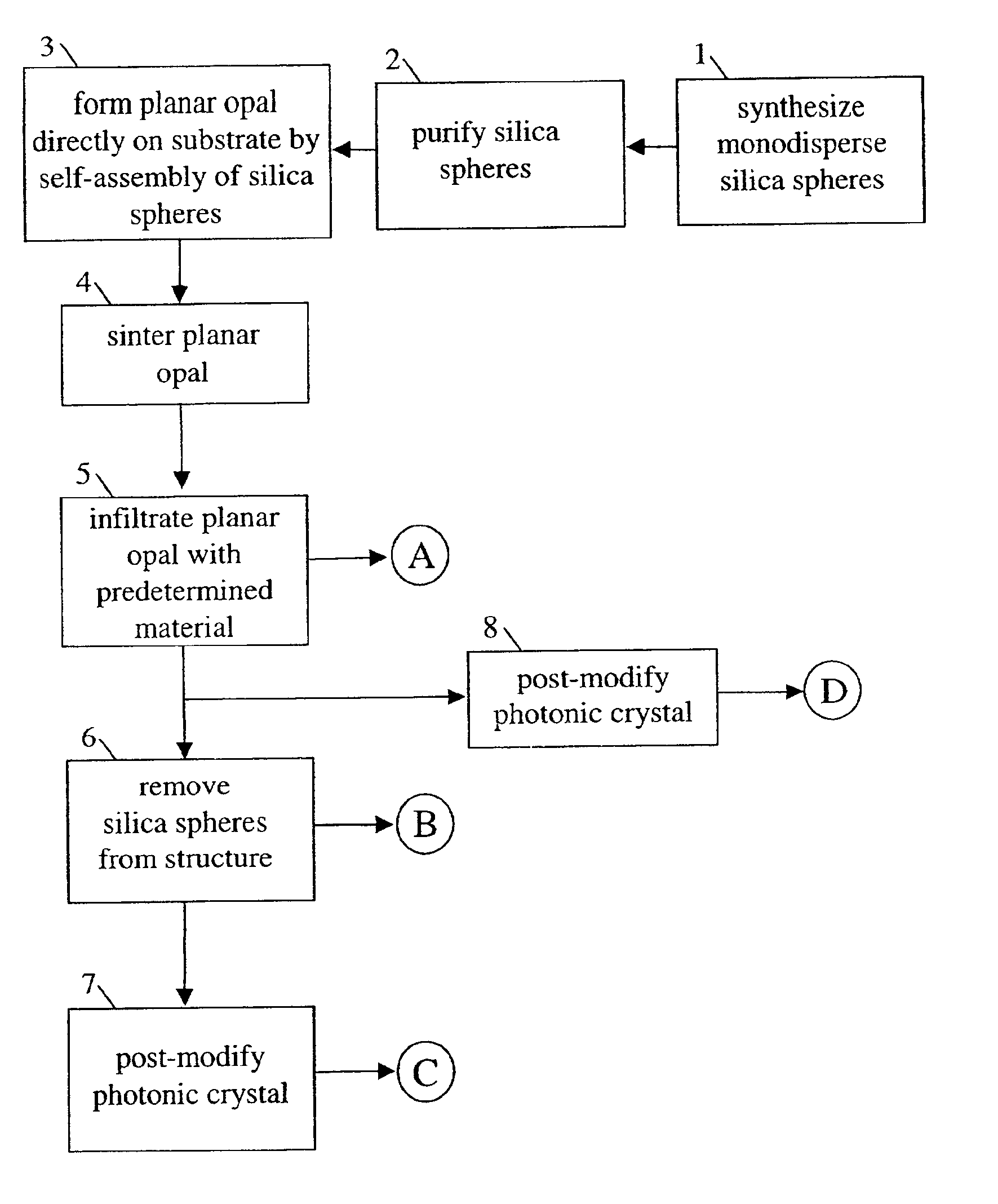
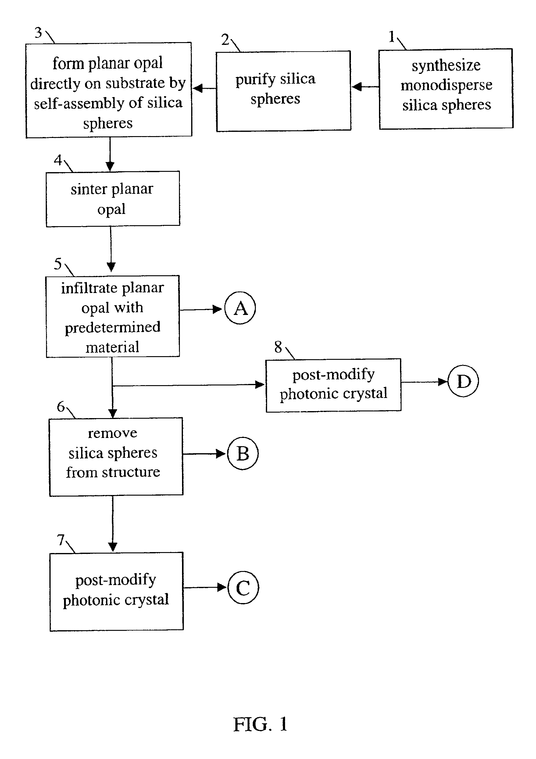
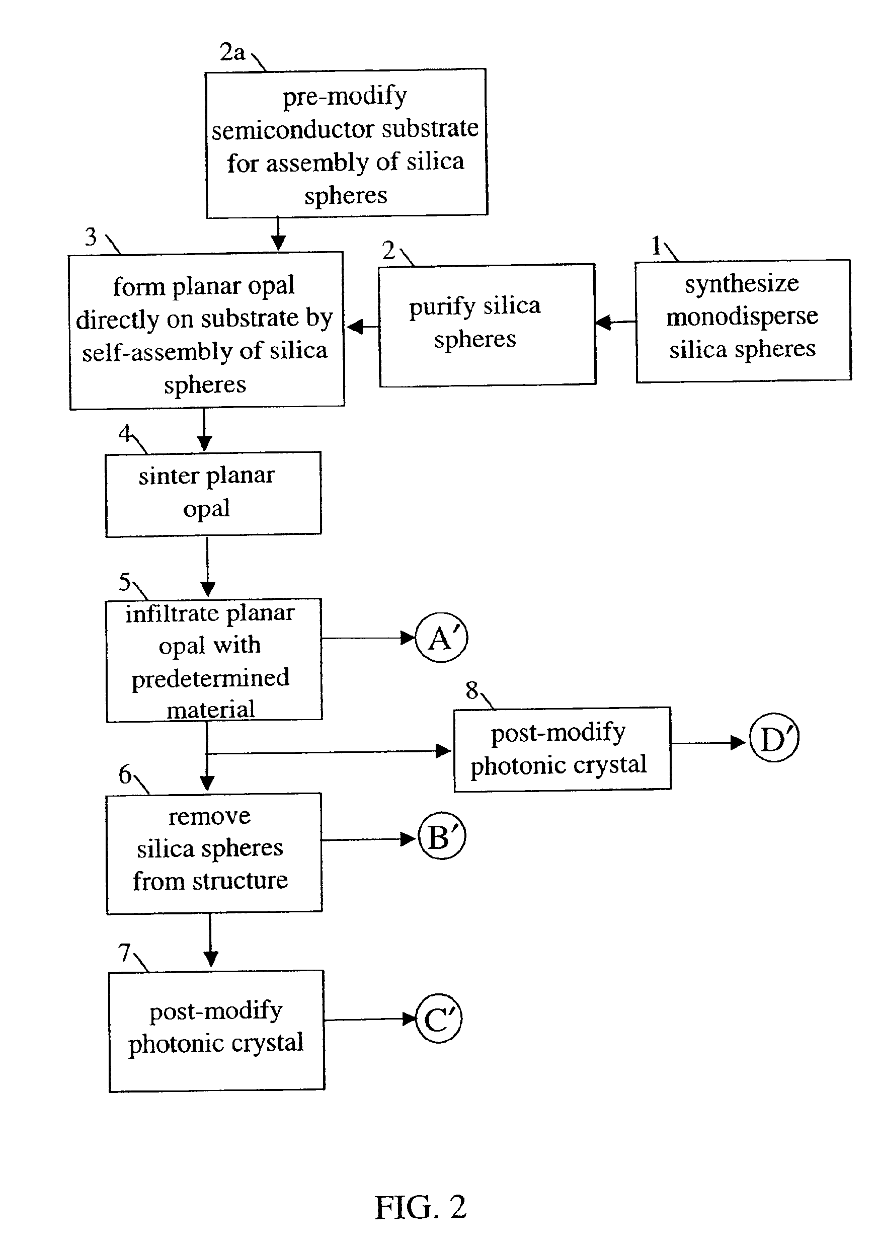
Examples
example 1
In this example, a large sphere planar opal is fabricated directly on a silicon wafer and then infiltrated with amorphous silicon using the “low pressure chemical vapor deposition” technique (LP-CVD). After conversion of the amorphous silicon to polycrystalline silicon with an annealing step, the result is a post-modified inverted planar opal composed of silicon and grown directly on a silicon wafer.
Synthesizing the Silica Spheres: Colloidal silica spheres, approximately 850 nm in diameter, can be synthesized according to standard methods. A typical synthesis begins by soaking all necessary chemical glassware in 5% aqueous hydrofluoric acid for approximately 30 minutes and then rinsing the glassware with filtered and deionized ultrapure water. To prepare for the reaction, the following are mixed in a large pre-cleaned glass vessel: 1 liter of filtered, anhydrous, 200 proof ethanol; 126 mL of filtered and deionized ultrapure (that is, 18 MOhm) water; and 167 mL of filtered aqueous am...
example 2
In this example, a silicon infiltrated planar opal is patterned by using conventional photolithography and RIE. The result is a post-modified inverted planar opal composed of silicon this is patterned for a desired application.
After a silicon infiltrated planar opal of desired thickness is obtained, as described in Example 1 above, the top layer of silicon is removed by RIE to expose the top layer of silica spheres. The structure is then spin-coated with a layer of photoresist, which is subsequently exposed with a Karl-Suss MA6 mask aligner. After developing the photoresist, the silica spheres are removed by immersing the sample in buffered HF (10%) for 1 hour. The result of these steps is a silicon inverted planar opal in which specific regions are masked by the photoresist. Anisotropic RIE is then used to remove the unmasked regions of the inverted planar opal. This is achieved with a PlasmaTherm 720 SLR RIE System operating with a flow of SF6 (60 sccm) and CCl2F2 (20 sccm) at a p...
example 3
In this example, a silicon infiltrated planar opal is patterned by using a slight modification of the procedure of Example 2. The result is a post-modified inverted planar opal composed of silicon that is patterned for a desired application.
After a planar silicon infiltrated opal of desired thickness is obtained, as described in Example 1, the top layer of silicon is removed by RIE to expose the top layer of silica spheres. The structure is then spin-coated with a layer of photoresist, which is subsequently exposed with a Karl-Suss MA6 mask aligner. After developing the photoresist, the sample is immersed in buffered HF (10%). However, in contrast to Example 2, the time of etching is carefully adjusted such that the silica spheres that are underneath the photoresist are not etched away while the spheres that are not covered by the photoresist are completely removed. This selectivity can be achieved since the spheres that are underneath the photoresist are much less accessible to the...
PUM
 Abstract
Description
Claims
Application Information