Conductive organic compound device, conductive liquid crystal device, and organic electroluminescence device

a technology of organic compound and conductive liquid crystal, which is applied in the direction of discharge tube luminescnet screen, natural mineral layered products, instruments, etc., can solve the problems of short circuit between the electrodes, difficult to provide a thickness in excess of 1 m in view of productivity, and increase the total thickness of the organic layer including the conductive liquid crystal layer. , the effect of reducing power consumption

Inactive Publication Date: 2005-02-22
CANON KK
View PDF8 Cites 31 Cited by
  • Summary
  • Abstract
  • Description
  • Claims
  • Application Information

AI Technical Summary

Benefits of technology

By using the conductive organic compound device or the conductive liquid crystal device having a carrier transporting layer exhibiting a high carrier injection efficiency, it is possible to constitute an electronic device requiring a reduced power consumption. According to the organic EL device of the present invention, the total thickness of the organic layers including the conductive liquid crystal layer can be increased, so that it is possible to provide a reliable EL device. Further, by forming a cell structure including a glass substrate, etc., it is possible to provide an

Problems solved by technology

The above-mentioned conventional organic EL devices involve a problem that a short circuit is liable to occur between the electrodes since a high electric field of approximately 100 mV/cm is applied across thin layers with a thickness of approximately 100 nm.
This problem can be alleviated to some extent by increasing the number of organic layers, but this can invite a problem in productivity.
An organic layer in a conventional organic EL device has been of a monomeric amorphous type and has been formed by vacuum evaporation, so that it has been difficult to provide a thickness in excess of 1 μm in view of the productivity.
Accordingly, the total thickness of the organic layers has generally been as thin as 100 nm-200 nm, and this has been accompanied with several problems.
More specifically, as the organic layers are thin, an electrical short circuit is liable to occur between the electrodes.
Further, due to the necessity of carrier injection, an insulating layer cannot be inserted, like it can in inorganic EL devices, to obviate the above problem.
As a result, the organic EL device has involved a problem regarding drive stability as an electronic device.
Further, as the organic layers between the electrodes are thin, the device capacitance is increased to cause a large drive current.
This incurs an increase in power consumption and is not desirable.
Moreover, as briefly mentioned above, in a conventional organic EL device, a high electric field (on the order of 10 V/100 nm) has been required for drive because of low performances of injection of electrons and holes from the electrodes, such as ITO, to the organic layers.
Therefore, organic materials are generally used in an amorphous state, but only a low carrier injection efficiency is available in this case.
The application of such a high electric field leads to the necessity of thin device layers, which also leads to an electrical short ci

Method used


Image

  • Conductive organic compound device, conductive liquid crystal device, and organic electroluminescence device
  • Conductive organic compound device, conductive liquid crystal device, and organic electroluminescence device
  • Conductive organic compound device, conductive liquid crystal device, and organic electroluminescence device

Examples


first embodiment

According to the present invention, an (electro)conductive organic compound having a π-electron resonance structure in its molecule is used to form a carrier transporting layer, wherein the π-electron resonance structure plane of the conductive organic compound is aligned substantially parallel to an associated electrode surface, thereby improving the carrier injection performance from the electrode boundary. A conductive organic compound device, particularly a conductive liquid crystal device using a conductive liquid crystal as the conductive organic compound, including such a carrier transporting layer, can be applied to electronic devices, such as a photo-sensor, a photoconductor (for constituting, e.g., a photosensitive drum for copying machines), an organic semiconductor device (such as an organic TFT (thin film transistor)), a temperature sensor, and a spatial modulation device, and is particularly preferable to an organic EL device.

If a conductive liquid crystal is used as t...

example 1

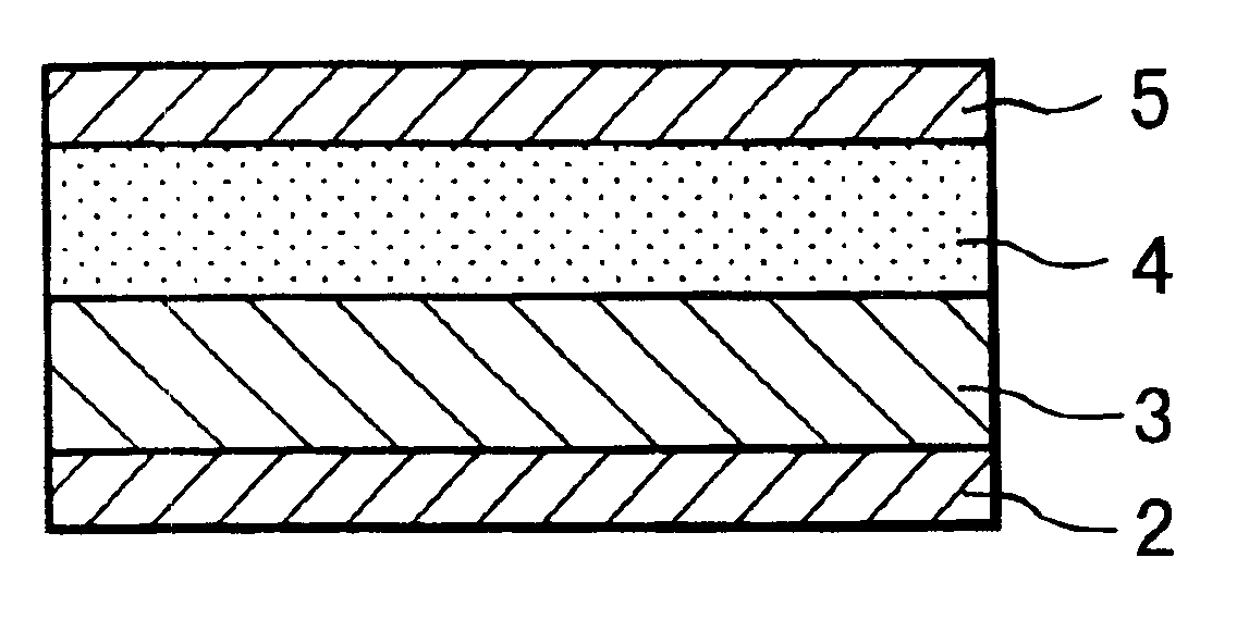
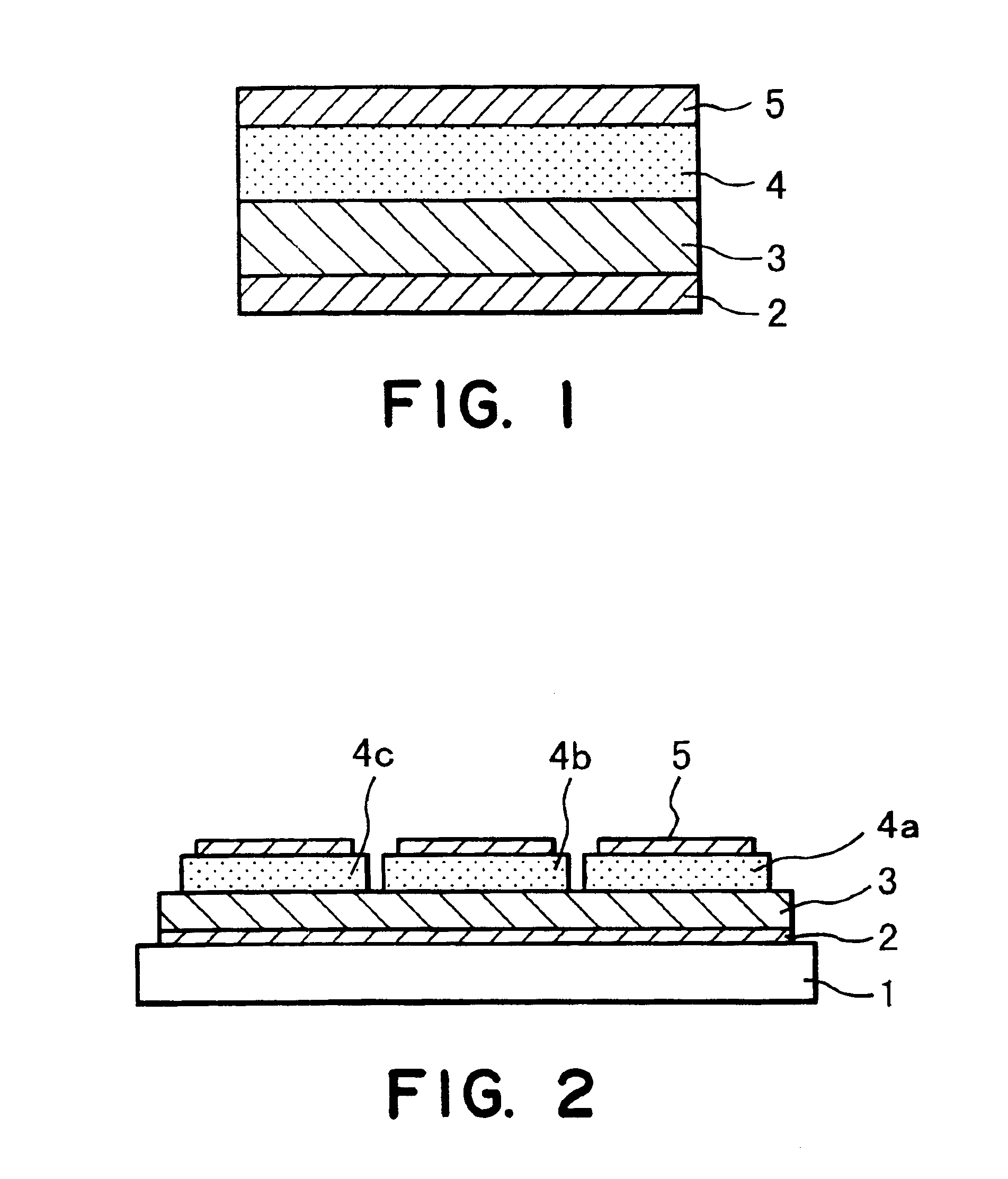
An organic EL device having a sectional structure as shown in FIG. 2 was prepared. FIG. 2 shows a similar structure as in FIG. 1 but shows a glass substrate 1 supporting the anode 2 and luminance layers 4a, 4b and 4c of different colors instead of the single luminance layer 4 in FIG. 1.

More specifically, on a glass substrate 1 held at 200° C., a 70 nm-thick ITO film was formed as a hole-injecting anode 2 by sputtering with a target of In 90% and Sn 10% while flowing Ar gas at 200 sccm and O2 gas at 3 sccm. The ITO film showing a work function of approximately 4.35 eV was exposed to ultraviolet rays from a low-pressure mercury lamp to have an elevated work function of 4.60 eV.

The above-treated substrate 1, having an ITO film 2, was placed in a vacuum chamber held at a pressure below 2×10⁻⁵ torr, and an approximately 50 nm-thick layer of HHOT (hexabishexyloxytriphenylene) was formed on the ITO film 2 as a carrier transporting layer 3 by vacuum deposition at a rate of approximately 0.1...

example 2

On a glass substrate, a 70 nm-thick ITO film was formed by sputtering similarly as in Example 1 and then subjected to an oxygen-plasma treatment under the conditions of O2 gas flow rate of 200 sccm, a pressure of 10 m.torr, a power of 400 W and a treatment time of 4 min., whereby the ITO film was caused to have an elevated work function of approximately 4.93 eV.

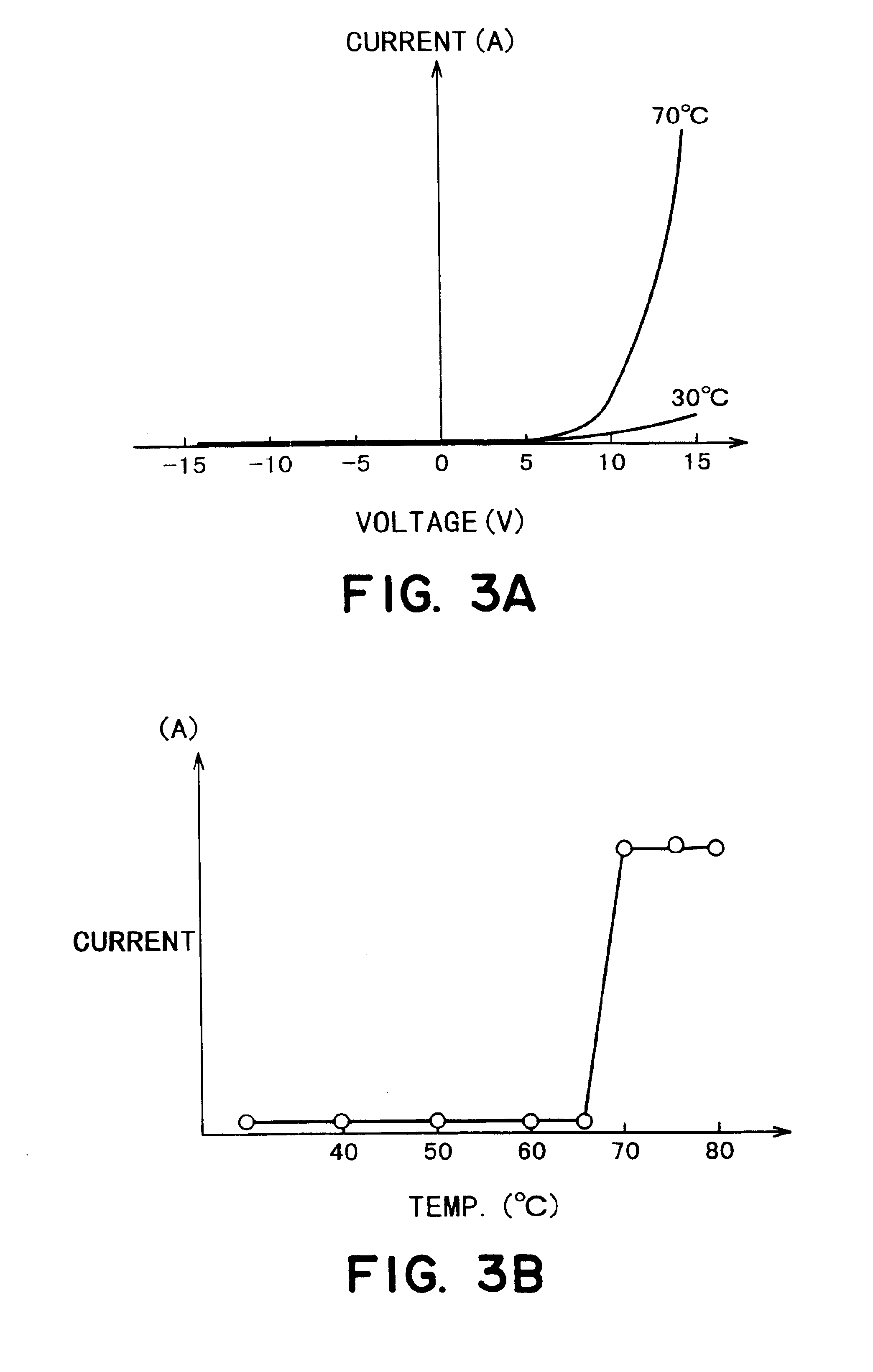
The above-treated substrate having an ITO film was coated with a carrier transporting layer comprising a lamination of a 20 nm-thick HHOT layer and a 50 nm-thick HBOT layer. The HHOT layer and the HBOT layer were respectively formed by the resistance heating vacuum deposition method at a pressure of 1×10⁻⁵ torr and a deposition rate of approximately 0.1 mm / sec successively in the same vacuum chamber with an intermediate re-evacuation step. HBOT exhibited a mobility of 1×10⁻² cm2 / V.sec at approximately 70° C. or below according to the time-of-flight method. HBOT is a discotic liquid causing a transition from crystal to discoti...


PUM

PropertyMeasurementUnit
Temperatureaaaaaaaaaa

Abstract

A conductive organic compound device structure suitable for constituting an electronic device, such as an organic EL device, is formed by including a pair of oppositely spaced electrodes, and a carrier transporting layer disposed between the electrodes and in contact with one of the electrodes. The carrier transporting layer comprises a conductive organic compound having a π-electron resonance structure in its molecule. In the device, the π-electron resonance structure plane of the conductive organic compound in the carrier transporting layer is aligned substantially parallel to surfaces of the electrodes. The conductive organic compound is preferably a conductive liquid crystal, such as a discotic liquid crystal or a smectic liquid crystal, and a layer thereof is included in the device, preferably by vacuum deposition.

Description

FIELD OF THE INVENTION AND RELATED ARTThe present invention relates to an (electro)conductive organic compound device used in electronic devices, an (electro)conductive liquid crystal device, and an organic electroluminescence device using the liquid crystal device.As for organic electroluminescence devices (hereinafter, the term “electroluminescence” being sometimes abbreviated as “EL” according to a common usage in the field), carrier injection-type EL devices utilizing organic solids, such as anthracene single crystal, were studied in detail. These devices were of a single layer-type, but thereafter Tang, et al. proposed a lamination-type organic EL device comprising a luminescent layer and a hole transporting layer between a hole injecting electrode and an electron injecting electrode. The luminescence mechanism in these injection-type EL devices commonly includes stages of (1) electron injection from a cathode and hole injection from an anode, (2) movement of electrons and hole...

Claims


Application Information

Patent Timeline
IPC IPC(8): H01L51/50H01L51/30H01L51/05H01L51/00
CPCH01L51/0054H01L51/0076H01L51/5012H01L51/0051H01L51/0055H01L51/0059H01L51/0065Y10T428/10H01L51/0078Y10S428/917Y10T428/1055H01L51/0071C09K2323/04C09K2323/00H10K85/611H10K85/622H10K85/623H10K85/653H10K85/631H10K85/731H10K85/311H10K85/657H10K50/11
Inventor OKADA, SHINJIROTSUBOYAMA, AKIRANISHIDA, NAOYAMORIYAMA, TAKASHI
Owner CANON KK
Why Eureka
Try Eureka