Semiconductor memory device
- Summary
- Abstract
- Description
- Claims
- Application Information
AI Technical Summary
Benefits of technology
Problems solved by technology
Method used
Image

Examples
example 1
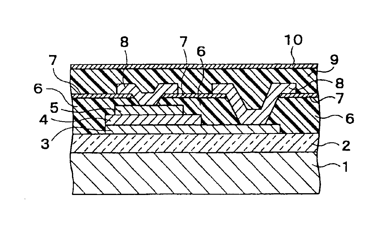
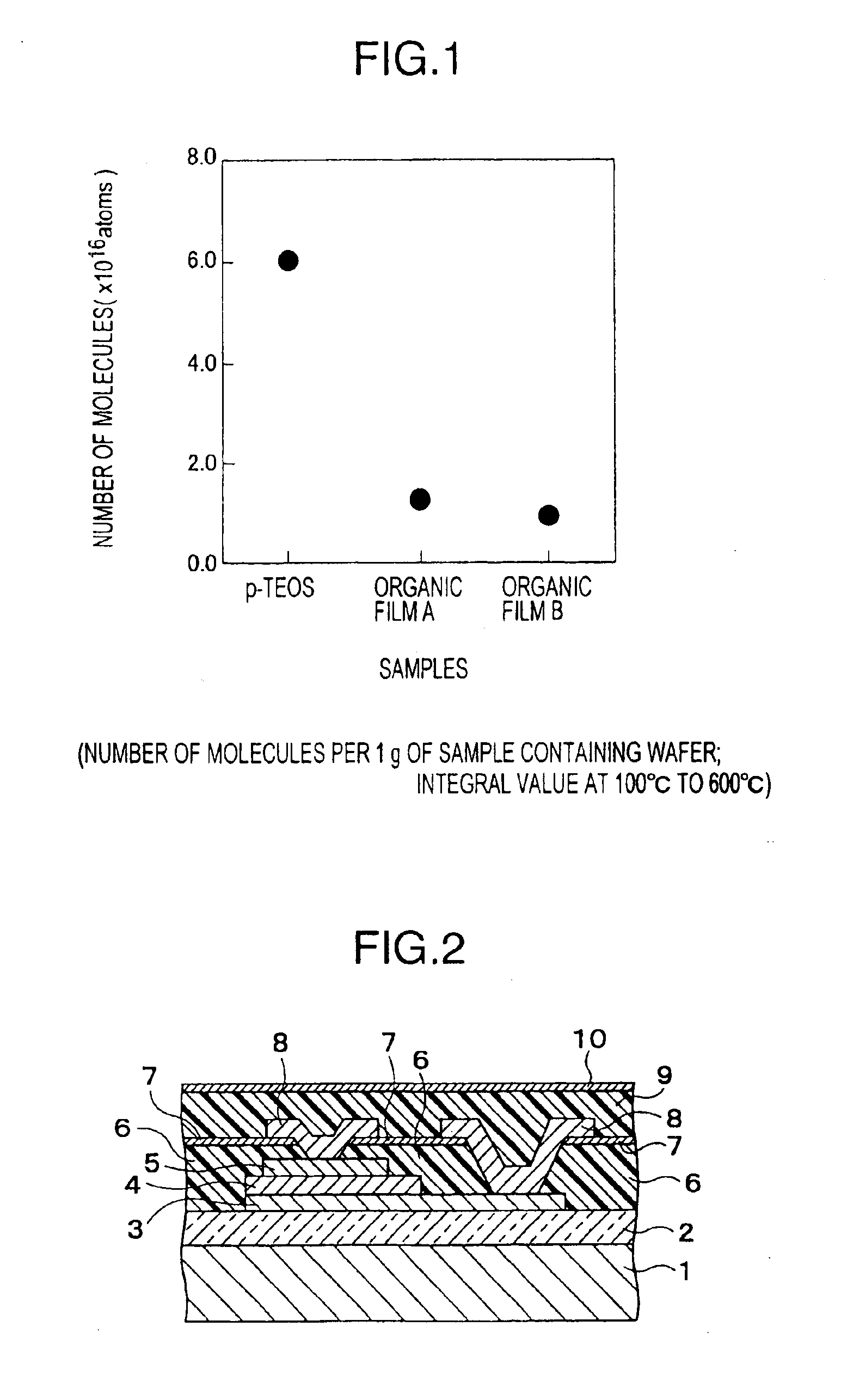
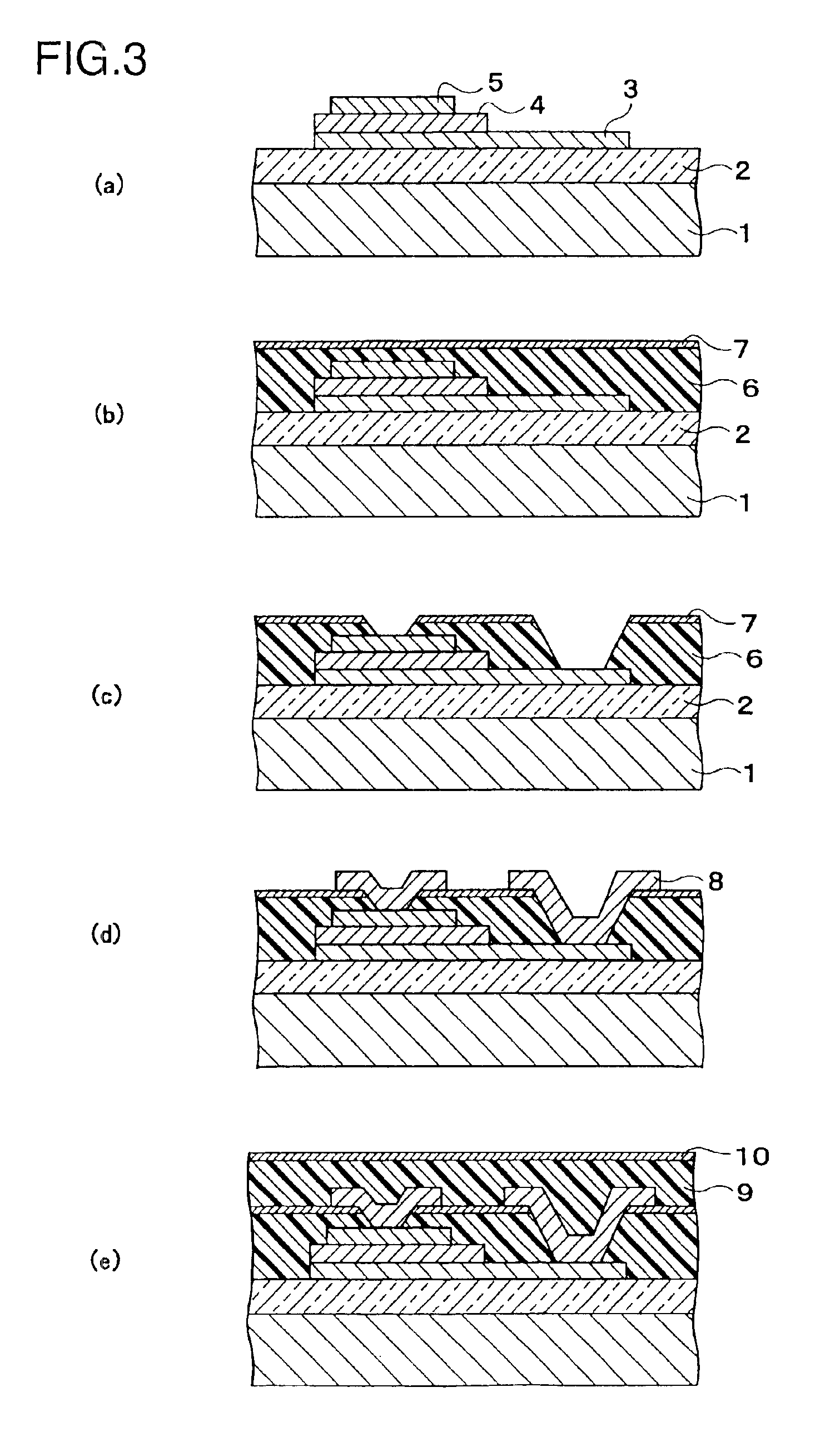
Example 1 is described with reference to the FIG. 3 flow sheet. A semiconductor wafer member is prepared which has a semiconductor substrate 1 on which transistors (not shown) have been fabricated, an interlayer insulation film 2 formed at the upper part thereof, and formed thereon a capacitor layer consisting of a lower electrode 3, a capacitive insulation film (ferroelectric layer) 4 and an upper electrode 5 (Step a).
On this wafer member, an organic insulation film material SILK (trademark; available from Dow Chemical) is coated by means of a spinner, a well known means, followed by heat treatment subsequently on hot plates of 180° C. and 320° C. for 1 minute each, and further followed by heat curing on a 430° C. hot plate for 10 minutes in a stream of nitrogen to form a first insulation film 6 (layer thickness: 400 nm). Next, on the first insulation film 6 thus formed, a TiO2 film (layer thickness: 50 nm) is vacuum-deposited as a second insulation film 7 by reactive sputtering at...
example 2
An example of a semiconductor memory device in which the multilayered film consisting of an organic film and a hard-mask material film is used in an interlayer insulation film formed between a capacitor layer making use of a ferroelectric film and a wiring layer formed at the upper part of the capacitor is cross-sectionally shown in FIG. 4.
On the same semiconductor device wafer member as that used in Example 1, an organic insulation film material FLARE (trademark; available from Honeywell) is spin-coated, followed by heat treatment subsequently on hot plates of, e.g., 150° C., 200° C. and 250° C. for 1 minute each. The coating film thus formed is subjected to heat curing on a 425° C. hot plate for 10 minutes in an atmosphere of nitrogen to form a first insulation film 6. Here, the first insulation film 6 is in a thickness of 500 nm.
Next, on the first insulation film 6 thus formed, a lead titanate zirconate [Pb(Zr,Ti)O3; abbreviation: PZT] film is formed by sol-gel processing. More s...
example 3
As a third embodiment of the present invention, a semiconductor memory device in which a second wiring is used in the region of a peripheral circuit is cross-sectionally shown in FIG. 5.
In the same manner as in Example 1, on a semiconductor wafer on which transistors, an interlayer insulation film 2 formed at the upper part thereof and a capacitor layer consisting of a lower electrode, a ferroelectric layer and an upper electrode have been formed, a first insulation film 6 and a second insulation film 7 are successively formed, and thereafter the second insulation film 7 is patterned. Subsequently, openings are formed in the first insulation film 6. Then, an upper Al wiring layer 8 formed thereon is subjected to etching to form an Al wiring pattern.
Next, as an interlayer insulation film, an SiO2 film 12 (layer thickness: 400 nm) is deposited by O3-TEOS CVD. Thereafter, through-holes for forming the wiring of the peripheral circuit are formed using a photoresist as a mask, by RIE (re...
PUM
 Abstract
Description
Claims
Application Information
 - R&D
- Intellectual Property
- Life Sciences
- Materials
- Tech Scout
- Unparalleled Data Quality
- Higher Quality Content
- 60% Fewer Hallucinations
Browse by: Latest US Patents, China's latest patents, Technical Efficacy Thesaurus, Application Domain, Technology Topic, Popular Technical Reports.
© 2025 PatSnap. All rights reserved.Legal|Privacy policy|Modern Slavery Act Transparency Statement|Sitemap|About US| Contact US: help@patsnap.com