Optoelectronic packaging substrate and production method of the same
a technology of optoelectronic packaging and substrate, which is applied in the direction of optical elements, circuit optical details, instruments, etc., can solve the problems of poor adhesion strength of metal patterns, no practicable metal patterns can be formed, and it is extremely difficult to use polysilane for electronic materials especially when reliability is required, and achieves excellent smoothness and high patterning precision. , the effect of simple process
- Summary
- Abstract
- Description
- Claims
- Application Information
AI Technical Summary
Benefits of technology
Problems solved by technology
Method used
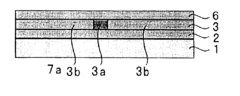
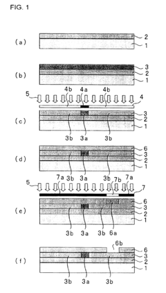
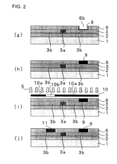
Image

Examples
examples
[0095]The branched type polysilane obtained in the above-mentioned synthesis example 100 parts by weight, DC-3037 (methylphenylmethoxysilicone resin, produced by Dow Corning Corp.) 50 parts by weight, and BTTB (3,3′,4,4′-tetra-(tert-butylperoxycarbonyl)benzophenone, produced by Nippon Oil & Fats Co., Ltd.) 15 parts by weight were dissolved in toluene 1,215 parts by weight to produce a photosensitive resin composition. The photosensitive resin composition was applied in a thickness of 20 μm to a glass substrate by using a spin coater, dried at 120° C. for 10 minutes in an oven, further dried at 200° C. for 30 minutes and 300° C. for 30 minutes to form a lower clad layer with a refractive index of 1.54.
[0096]Next, branched type polysilane obtained in the above-mentioned synthesis example 100 s part by weight, DC-3074 (methylphenylmethoxysilicone resin, produced by Dow Corning Corp.) 50 parts by weight, and BTTB 15 parts by weight were dissolved in toluene 1,215 s part by weight to pro...
PUM
| Property | Measurement | Unit |
|---|---|---|
| Percent by mass | aaaaa | aaaaa |
| Percent by mass | aaaaa | aaaaa |
| Percent by mass | aaaaa | aaaaa |
Abstract
Description
Claims
Application Information