Plasma ashing process

a technology of ashing process and plasma, which is applied in the field of plasma ashing process, can solve the problems of adversely affecting device performance, yield and reliability of the final integrated circuit, and oxygen-containing plasmas readily damage certain materials used in advanced integrated circuit manufacturing, and achieve the effect of increasing the ashing ra

Inactive Publication Date: 2005-10-04
LAM RES CORP
View PDF21 Cites 40 Cited by
  • Summary
  • Abstract
  • Description
  • Claims
  • Application Information

AI Technical Summary

Benefits of technology

[0063]The foregoing descriptions of the preferred embodiments of the disclosure have been presented for purposes of illustration and description. It is not intended to be exhaustive or to limit the disclosure to the precise forms disclosed. Obvious modifications or variations are possible in light of the above teachings. The embodiments were chosen and described to provide the best illustration of the principles of the disclosure and its practical applications to thereby enable one of ordinary skill in the art to utilize the disclosure in various embodiments and with various modifications as are suited to the particular use contemplated. All such modifications and variations are within the scope of the disclosure as determined by the appended claims when interpreted in accordance with the breadth to which they are fairly, legally and equitably entitled.

Problems solved by technology

Small deviations in the patterned profiles formed in the underlayers can adversely impact device performance, yield and reliability of the final integrated circuit.
However, it has been found that oxygen-containing plasmas readily damage certain materials used in advanced integrated circuit manufacture.
The increases in dielectric constant affects, among others, interconnect capacitance, which directly impacts device performance.
Moreover, the use of oxygen-containing plasmas is generally less preferred for advanced device fabrication employing copper metal layers.
However, in some cases, it has been found that the use of oxygen-free plasmas containing nitrogen may alter and / or affect the chemical, mechanical and electrical properties of the underlying substrate.
For example, exposing carbon and / or hydrogen containing low k dielectric materials to oxygen-free plasma generated from hydrogen, nitrogen and fluorine gas mixtures results in significant damage.
Occasionally, the damage is not detected during metrology inspection of the substrate after plasma processing.
However, the damage can be readily demonstrated by a subsequent wet cleaning process, as may be typically employed after plasma ashing, wherein portions of the carbon and / or hydrogen-containing low k dielectric material are removed.
The removed portions of the dielectric material are a source of variation in the critical dimension (CD) of the feature that is frequently unacceptable and impacts overall device yield.
Moreover, even if a wet clean process is not included, the electrical and mechanical properties of the dielectric material may be changed by exposure to the oxygen-free plasmas thereby affecting operating performance.
Since oxygen-free plasmas are normally generated from gas mixtures that contain nitrogen, it is believed that nitrogen damages the dielectric in such a way that it causes problems during subsequent metal filling processes, such as the creation of voids at the bottom of trench structures.

Method used


Image

  • Plasma ashing process
  • Plasma ashing process
  • Plasma ashing process

Examples


example 1

[0045]As illustrated by this example, a significant advantage of the oxygen-free and nitrogen-free plasma process is the improvement in removal efficiency of photoresist, organic overlayers, and polymers / residues from substrates including carbon containing low k dielectrics without affecting the underlying dielectric layers. This is a significant commercial advantage as device manufacturers transition to the use of low k dielectric layers in the fabrication of advanced integrated circuits.

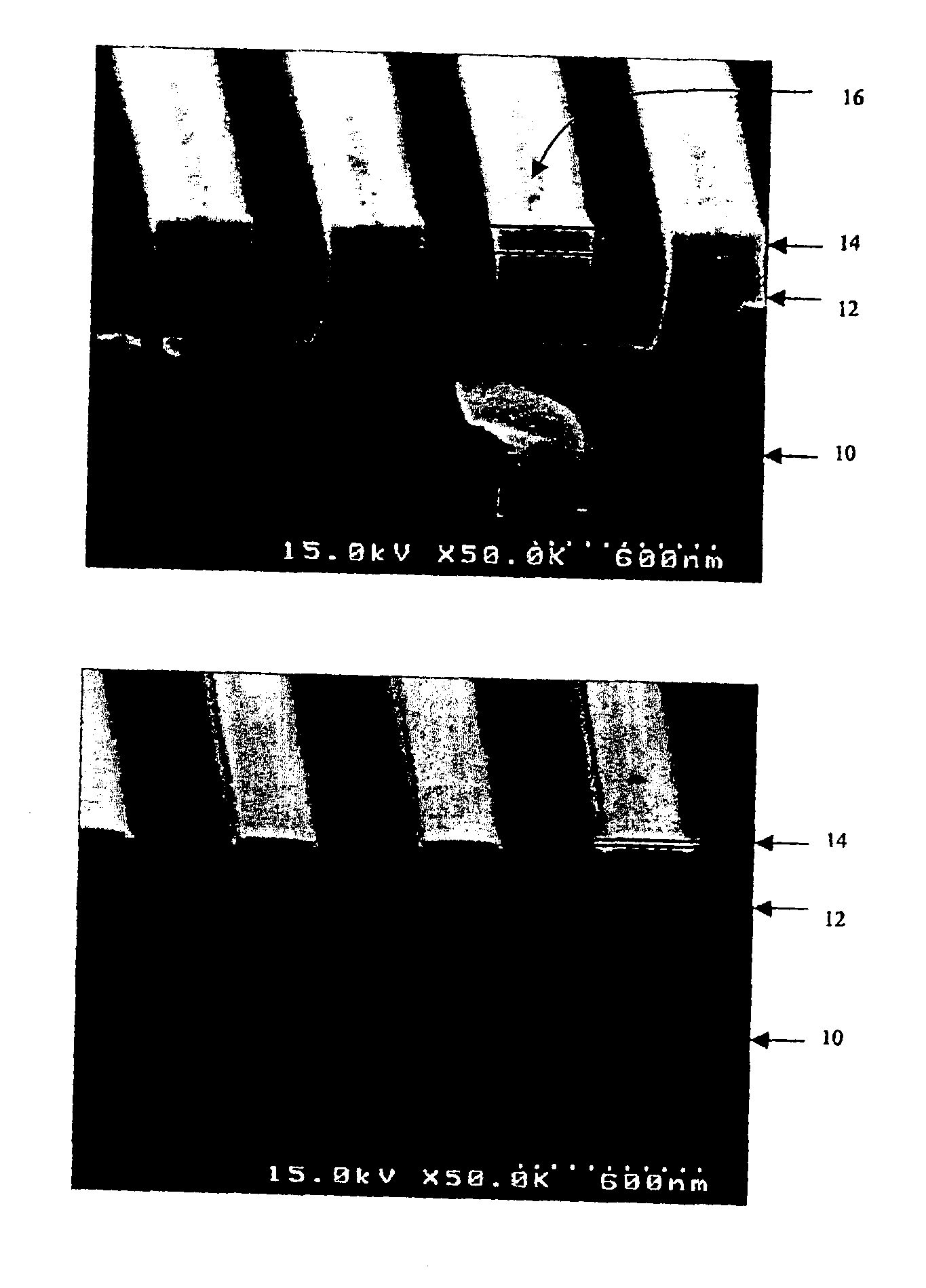
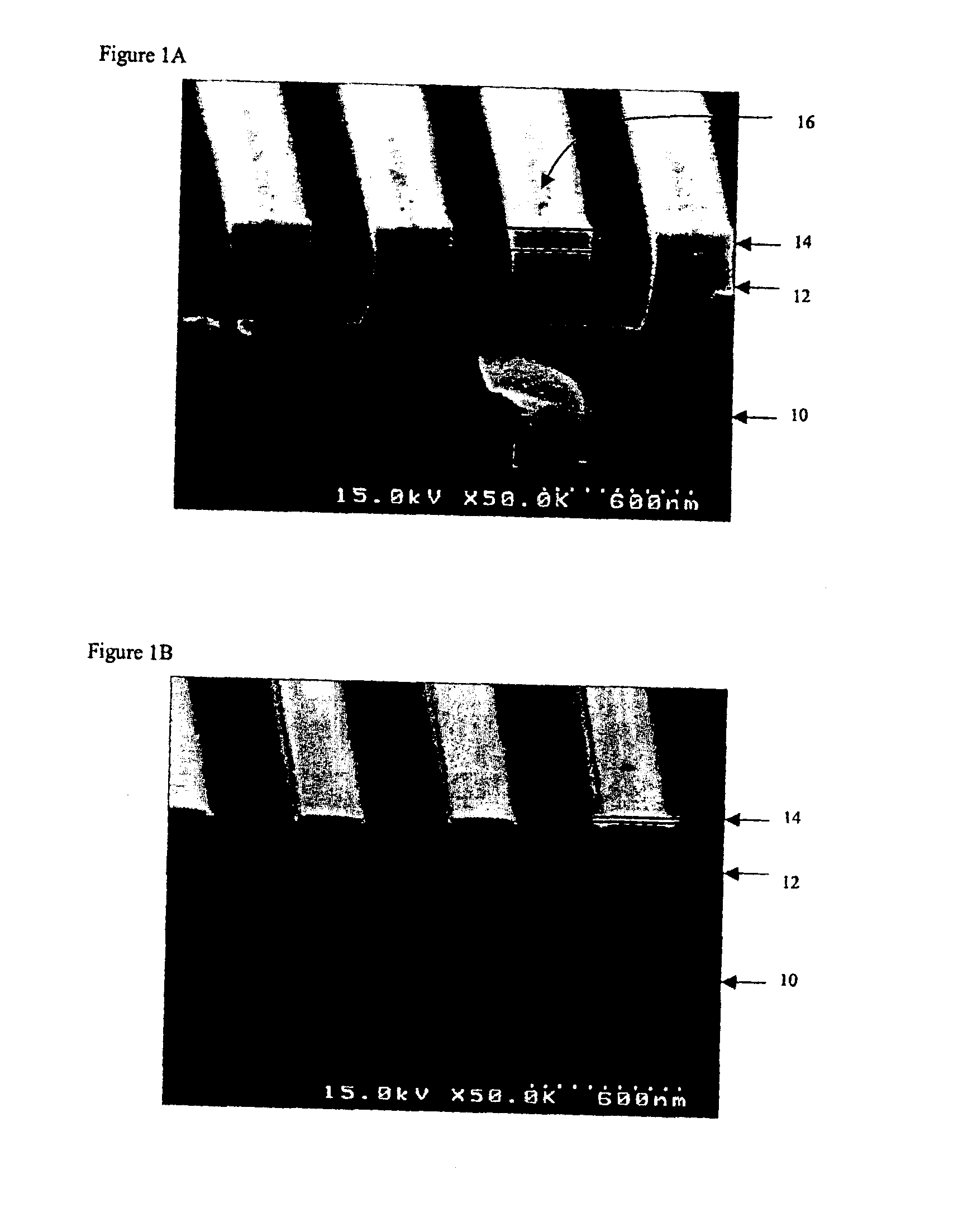
[0046]Referring now to FIGS. 1A and 1B, trench patterns were etched into multiple silicon substrates 10 by an etcher using standard etching processes. The substrates 10 included a low k dielectric layer 12 and a silicon dioxide layer 14. The patterns were selectively etched by use of a patterned I-line photoresist mask. The low k dielectric layer 12 was a carbon-doped oxide commercially available under the trade name CORAL. The substrates were then ashed using a Fusion Gemini ES3 Plasma Asher avail...

example 2

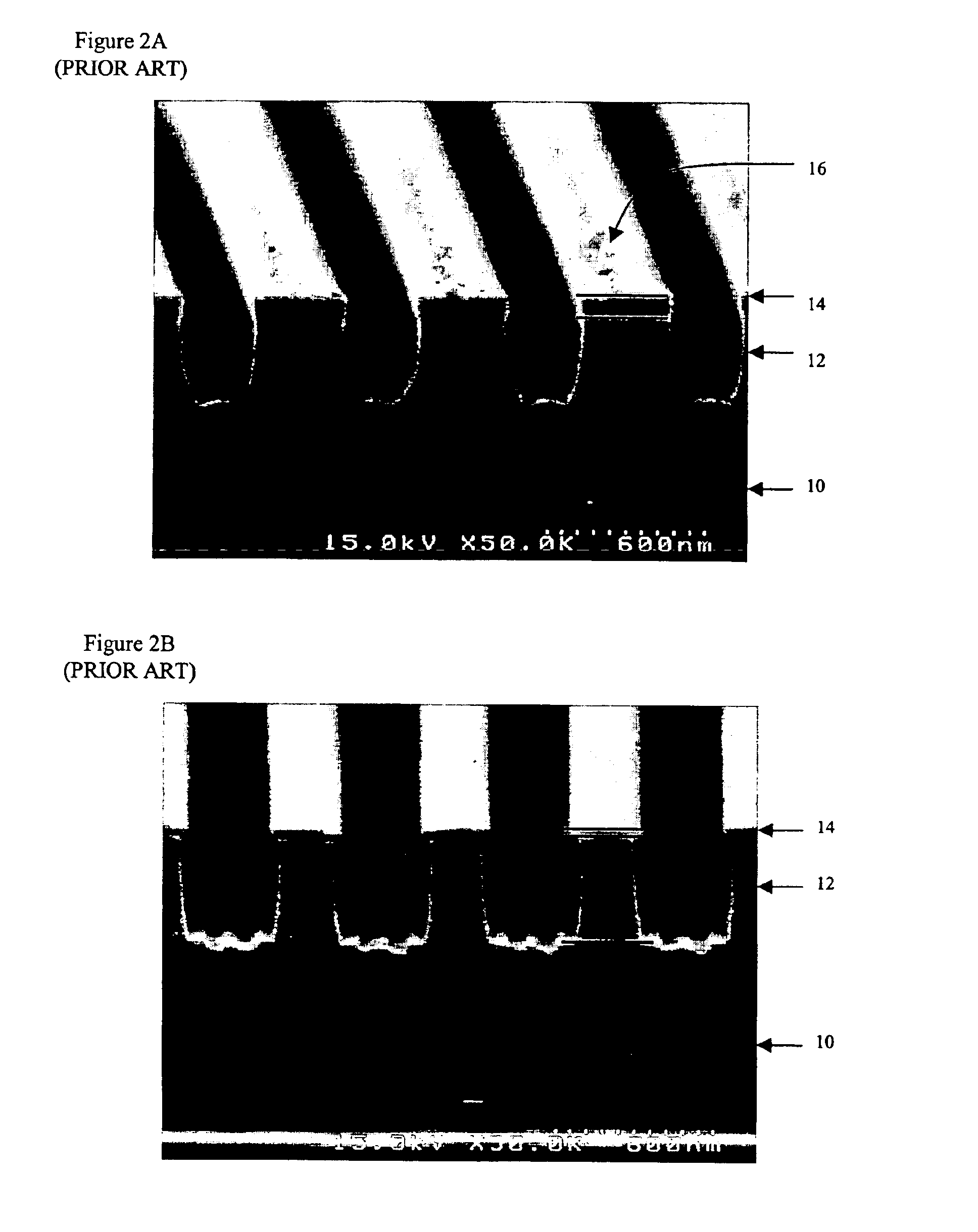
[0049]In this example, the substrates were prepared in accordance with Example 1 and exposed to a conventional ashing plasma process. The plasma gas mixture included nitrogen gas in place of the helium gas and at the same volume percentage. All other conditions were identical to that in Example 1. The process conditions are shown in Table II.

[0050]

TABLE IINitrogen-containing PlasmaTimePressurePower5% H2 / N2CF4 Step(min.)(torr)(W)Temp (° C.)(sccm)(sccm)1251.5Off3705000502201.51500370500050

[0051]As shown in FIG. 2A, scanning electron microscopy of substrates ashed with the nitrogen-containing plasma yielded results similar to the nitrogen-free plasma process of Example 1. A comparison of FIGS. 1A and 2A show similar etch profiles. However, as shown in FIG. 2B, exposing the ashed wafers to the same wet clean process used in Example 1 resulted in significant CD loss of the low k dielectric layer 12. The wet clean process clearly removed significant amounts of the low k dielectric materia...

example 3

[0052]In this example, the rate of photoresist removal was monitored as a function of the percentage of hydrogen gas in the plasma. Substrates were coated with a thick layer of photoresist and exposed to one of four different plasmas (A-D) in a Fusion Gemini ES3 plasma asher. The process conditions and flow rates were held constant for each wafer set. The photoresist thickness was conventionally measured by ellipsometry before and after processing in order to determine the removal rate. As shown in Table III, the substrates were exposed to: A. a nitrogen-free plasma, B. a nitrogen-free plasma with tetrafluoromethane (CF4), C. a nitrogen-containing plasma and D. a nitrogen-containing plasma with CF4. The percentage of hydrogen in the plasma gas mixture was varied as a percentage of the total volume of the hydrogen gas mixture. The results are graphically shown in FIG. 3.

[0053]

TABLE IIIPlasma Gas CompositionsHydrogen / Nitrogen(FORMING GAS)Hydrogen / HeliumCF4PLASMAflow rate (sccm)flow ra...


PUM

PropertyMeasurementUnit
dielectric constantaaaaaaaaaa
temperatureaaaaaaaaaa

Abstract

A substantially oxygen-free and nitrogen-free plasma ashing process for removing photoresist in the presence of a low k material from a semiconductor substrate includes forming reactive species by exposing a plasma gas composition to an energy source to form plasma. The plasma gas composition is substantially free from oxygen-bearing and nitrogen-bearing gases. The plasma selectively removes the photoresist from the underlying substrate containing low k material by exposing the photoresist to substantially oxygen and nitrogen free reactive species. The process can be used with carbon containing low k dielectric materials.

Description

CROSS REFERENCE TO RELATED APPLICATIONS[0001]The present disclosure is a continuation-in-part application of, and claims is priority to, U.S. patent application Ser. No. 09 / 855,177, filed on May 14, 2001, now U.S. Pat. No. 6,630,406, incorporated herein by reference in its entirety.BACKGROUND[0002]The present disclosure relates generally to plasma ashing processes for selectively removing photoresist, organic overlayers, and polymer residues from a substrate surface, and in particular, to a substantially oxygen-free and nitrogen-free plasma ashing process.[0003]Ashing is a plasma mediated stripping process by which photoresist, organic overlayers, and / or polymer residues are stripped or removed from a substrate upon exposure to the plasma. Ashing generally occurs after an etching process has been performed in which the photoresist material is used as a photomask for etching a pattern into the substrate. The ashing process is also used to remove other organic layers such as the anti-...

Claims


Application Information

Patent Timeline
Patent Type & Authority Patents(United States)
IPC IPC(8): H01L21/02H01L21/3213H01L21/311G03F7/42
CPCG03F7/427H01L21/31138H01L21/02071H01J2237/3342H01L21/02057
Inventor WALDFRIED, CARLOESCORCIA, ORLANDOHAN, QINGYUANBUCKLEY, THOMASSAKTHIVEL, PALANI
Owner LAM RES CORP
Why Eureka
Try Eureka