Plasma producing apparatus and doping apparatus

a plasma producing apparatus and plasma technology, applied in plasma techniques, nanoinformatics, coatings, etc., can solve the problems of reducing throughput, short lifespan of filaments, and lowering apparatus availability, so as to achieve high density plasma production, stable plasma, and superior heat resistance and current transport

Inactive Publication Date: 2006-04-11
SEMICON ENERGY LAB CO LTD
View PDF30 Cites 15 Cited by
  • Summary
  • Abstract
  • Description
  • Claims
  • Application Information

AI Technical Summary

Benefits of technology

[0017]When plasma is thus produced using the cathode electrode where carbon nano tubes are formed, high density plasma can be obtained efficiently. In addition, superior heat resistance and current transporting characteristic of carbon nano tubes make it possible to produce stable plasma in an ion source. Then, an ion doping apparatus, etching apparatus, sputter apparatus, and film forming apparatus each having such a cathode electrode can be used to perform a variety of stable processes on a semiconductor film.

Problems solved by technology

A problem of the ion doping apparatus with a DC ion source using a filament is that a filament has a short lifespan.
Replacing a filament lowers the availability of the apparatus and reduces the throughput.
In addition, it is desirable to replace a filament as less frequently as possible because many ion doping apparatuses use phosphine, diborane, and other harmful gas for material gas and it can contaminate a clean room and adversly affect human health.
These changes in a filament cause a change with time in field emission characteristic from the filament surface and a change in ion species ratio in plasma, thereby making stable dose control impossible.

Method used


Image

  • Plasma producing apparatus and doping apparatus
  • Plasma producing apparatus and doping apparatus
  • Plasma producing apparatus and doping apparatus

Examples


embodiment mode 1

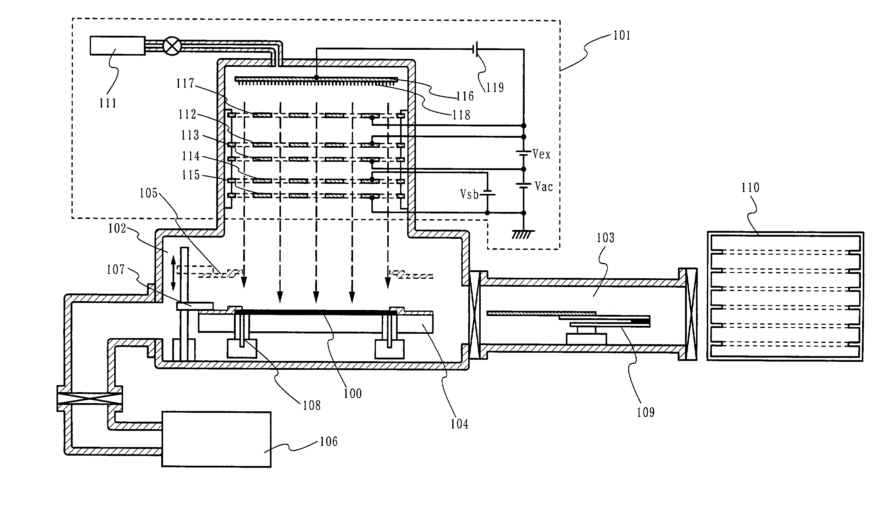
[0024]This embodiment describes with reference to FIG. 1 a plasma producing apparatus having a cathode electrode and an anode electrode.

[0025]FIG. 1 shows an example of a plasma producing apparatus of the present invention. In FIG. 1, a chamber is equipped with a plasma chamber 101, a processing chamber 102, a load lock chamber 103, vacuum exhaust means 106, a gas supplying system 111, a cathode electrode 116 for producing plasma, and an anode electrode 117. The structure in FIG. 1 conforms to the capacitively coupled high frequency electric discharge format. Instead, a filament type electrode may be used.

[0026]A carbon nano tube 118 to serve as an electron emission source is formed on a metal member of the cathode electrode 116. The carbon nano tube 118 is manufactured by arc discharge or laser irradiation to graphite and refined before being bonded to the metal member with a conductive paste. In particular, a carbon nano tube obtained by arc discharge has excellent crystallinity a...

embodiment mode 2

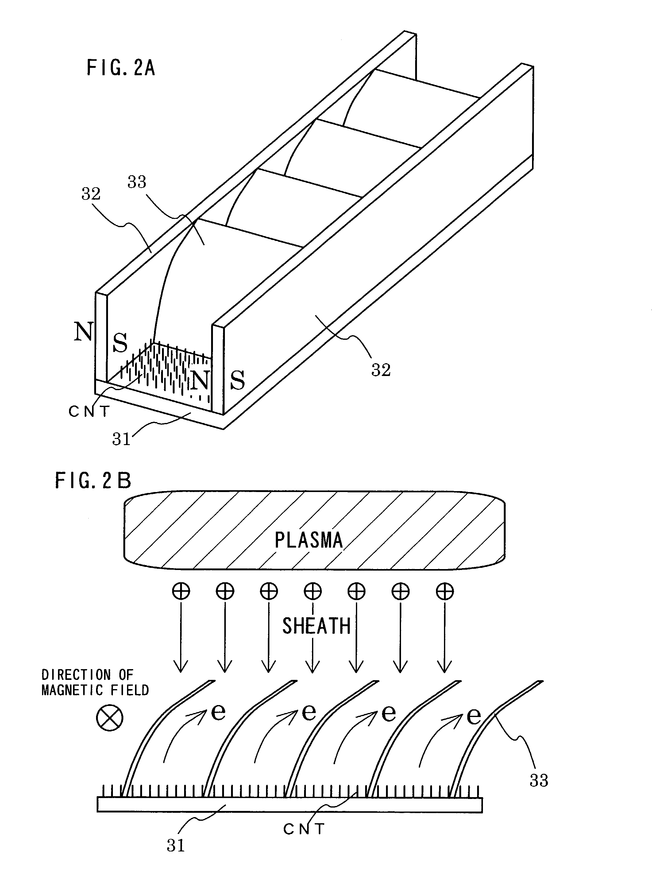
[0031]This embodiment describes with reference to FIGS. 2A and 2B a cathode electrode structure different from the one in Embodiment Mode 1. FIG. 2A is a bird's-eye view and FIG. 2B shows a section perpendicular to a magnetic field that is formed in parallel to a cathode electrode.

[0032]A cathode electrode 31 is composed of a metal member and a carbon nano tube formed on a surface of the metal member. Similar to Embodiment Mode 1, the carbon nano tube is manufactured by arc discharge or laser irradiation and refined before being bonded to the metal member with a conductive paste. Alternatively, the carbon nano tube is obtained through vapor phase growth directly on the metal member using plasma CVD.

[0033]A plate-like or rod-like magnet 32 is placed on each side of the cathode electrode 31 in a manner that makes the north pole and the south pole face each other. A plurality of blocking plates 33 are placed between the magnet 32 and the other magnet 32. The blocking plates 33 are each...

embodiment 1

[0038]This embodiment describes the present invention by taking a doping apparatus as an example and referring to FIG. 1.

[0039]Major components of the doping apparatus of FIG. 1 are an ion source 101, a processing chamber 102, a load lock chamber 103, and vacuum exhaust means 106. The processing chamber 102 is a place where a substrate is held and ions are implanted, and the chamber is provided with a substrate stage 104 and a damper 105. A pin 108 for moving a substrate up and down on the substrate stage is used when a substrate is put on the substrate stage 104 by transporting means 109 after the transporting means brings the substrate from the load lock chamber 103. The damper 105 is moved up and down by an arm 107 as the substrate is brought in and out.

[0040]With the clamper 105 lifted above the substrate stage by the arm 107, a substrate is brought in by the transporting means 109. At this point, the pin 108 is jetting out from the substrate stage 104 and a substrate 100 is pla...


PUM

PropertyMeasurementUnit
melting pointaaaaaaaaaa
diameteraaaaaaaaaa
energyaaaaaaaaaa

Abstract

An object of the present invention is to provide an apparatus for producing stable plasma. Another object of the present invention is to provide an apparatus having a long-lasting cathode electrode which is superior in field emission characteristic since the plasma density has to be raised in order to increase the throughput. The structure of the plasma producing apparatus of the present invention relates to a plasma producing apparatus with a plasma chamber surrounded by walls to make material gas into plasma, characterized in the plasma chamber has a cathode electrode, an anode electrode, means for introducing the material gas, and exhaust means, and that a carbon nano tube is formed on a surface of the cathode electrode and the anode electrode is formed on the surface of the cathode electrode.

Description

BACKGROUND OF THE INVENTION[0001]1. Field of the Invention[0002]The present invention relates to an apparatus for producing plasma of high density, and to apparatus that uses the same. For example, the plasma producing apparatus is employed in a doping apparatus, etching apparatus, sputtering apparatus, and film forming apparatus.[0003]2. Description of the Related Art[0004]In recent years, manufacture of a transistor from a thin film (thin film transistor: TFT) has been widely researched. In manufacture of a TFT, film formation, etching, and ion introduction are some of indispensable processes and plasma is often utilized in these steps. To be specific, highly reactive ions or radicals are utilized in etching and film formation, particles having large kinetic energy are utilized in sputtering, and charged particles in plasma are utilized in etching and ion implantation. A TFT is manufactured through these steps using sputtering, plasma CVD, etching, ion doping, and the like.[0005]T...

Claims


Application Information

Patent Timeline
Patent Type & Authority Patents(United States)
IPC IPC(8): H01J7/24H05H1/46H01J37/32H01L21/265H05H1/48
CPCB82Y10/00H01J37/3255H01J37/32009
Inventor NAKAMURA, OSAMU
Owner SEMICON ENERGY LAB CO LTD
Why Eureka
Try Eureka