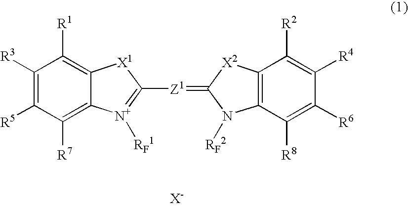
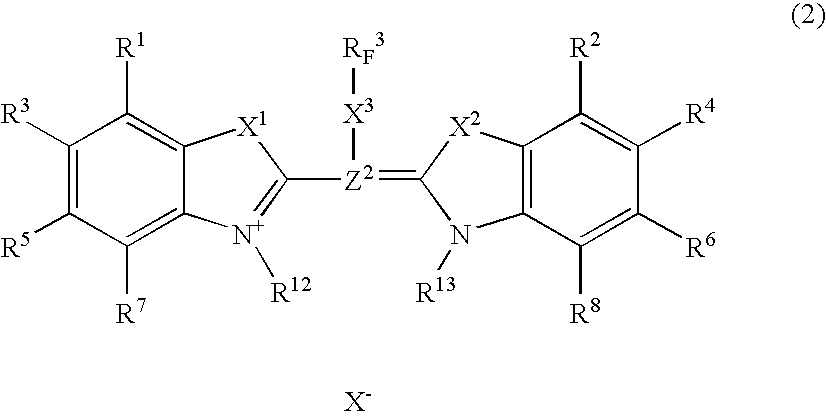
Image-formation material and infrared absorber
a technology of infrared absorber and material, which is applied in the direction of photosensitive materials, thermography, other chemical processes, etc., can solve the problems of insufficient utilization of energy for forming images, loss of solution inhibiting ability, and extensive thermal diffusion to a substrate, etc., and achieve excellent image-forming properties and high sensitivity
- Summary
- Abstract
- Description
- Claims
- Application Information
AI Technical Summary
Benefits of technology
Problems solved by technology
Method used
Image
Examples
example 1
Example of a Positive Image-Formation Material
[Production of Substrate]
[0235]An aluminum plate (material 1050) having a thickness of 0.3 mm was degreased by washing with trichloroethylene. Then, the surface thereof was grained using a nylon brush and a pumice-water suspension of 400 mesh, and washed thoroughly with water. This plate was immersed in a 25% aqueous sodium hydroxide solution at 45° C. for 9 seconds to effect etching, and washed with water, then further immersed in a 20% nitric acid solution for 20 seconds, and washed with water. The etched amount of the grained surface in this procedure was about 3 g / m2. Then, the plate was treated with a current density of 15 A / dm3 using 7% sulfuric acid as an electrolyte, to form thereon a direct current anodized film of 3 g / m2. Then, the plate was washed with water and dried, a primer solution described below was applied thereto, and the film was dried at 90° C. for 1 minute. The amount of the film applied after drying was 10 mg / m2.
[...
examples 2 and 3
[0239]Planographic printing plates [A-2] and [A-3] were obtained in the same manner as in Example 1 except that the infrared absorption agent compounded in the photosensitive layer coating solution [A] in Example 1 was replaced with the exemplary compounds described in the following table 1.
example 4
[0242]The following photosensitive layer coating solution [B] was applied to a substrate obtained in the same manner as in Example 1 such that a coating amount was 1.6 g / m2, to obtain a planographic printing plate [B-1].
(Photosensitive Layer Coating Solution [B])
[0243]
m,p-Cresol novolak (m / p ratio = 6 / 4, weight-average molecular 0.3 gweight 3,500, containing unreacted cresol 0.5% by weight)Copolymer 1 described in JP-A No. 11-348443 0.7 gBis(4-hydroxyphenyl)sulphone 0.1 gInfrared absorption agent (exemplary compound IR-5) 0.15 gp-Toluenesulfonic acid0.002 gDye obtained by setting counter ion in Victoria Pure Blue BOH 0.02 gto 1-naphthalenesulfonate anionFluorine-based nonionic surfactant (trade name: Megafac F-177, 0.05 gDainippon Ink & Chemicals Inc.)γ-Butyrolactone 8 gMethyl ethyl ketone 8 g1-Methoxy-2-propanol 4 g
PUM
| Property | Measurement | Unit |
|---|---|---|
| wavelength range | aaaaa | aaaaa |
| particle size | aaaaa | aaaaa |
| particle size | aaaaa | aaaaa |
Abstract
Description
Claims
Application Information


