

Low temperature method and composition for producing electrical conductors
a low temperature method and composition technology, applied in the field of compositions, can solve the problems of poor electrical conductivity, poor solderability, and connection to additive traces, and achieve the effect of reducing cost and speed
- Summary
- Abstract
- Description
- Claims
- Application Information
AI Technical Summary
Benefits of technology
Problems solved by technology
Method used
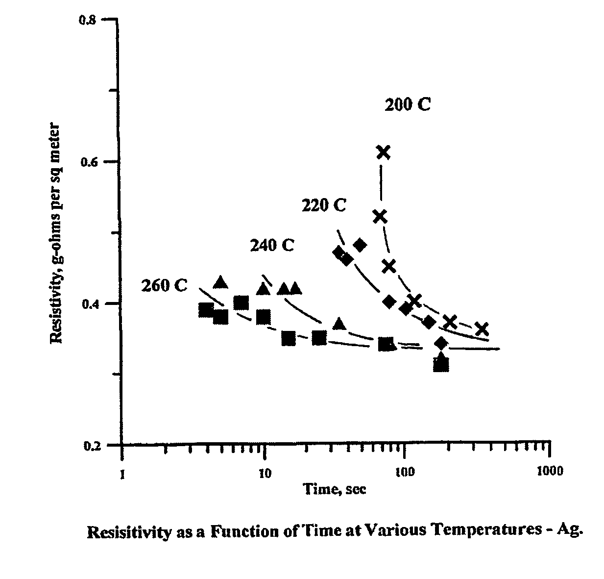
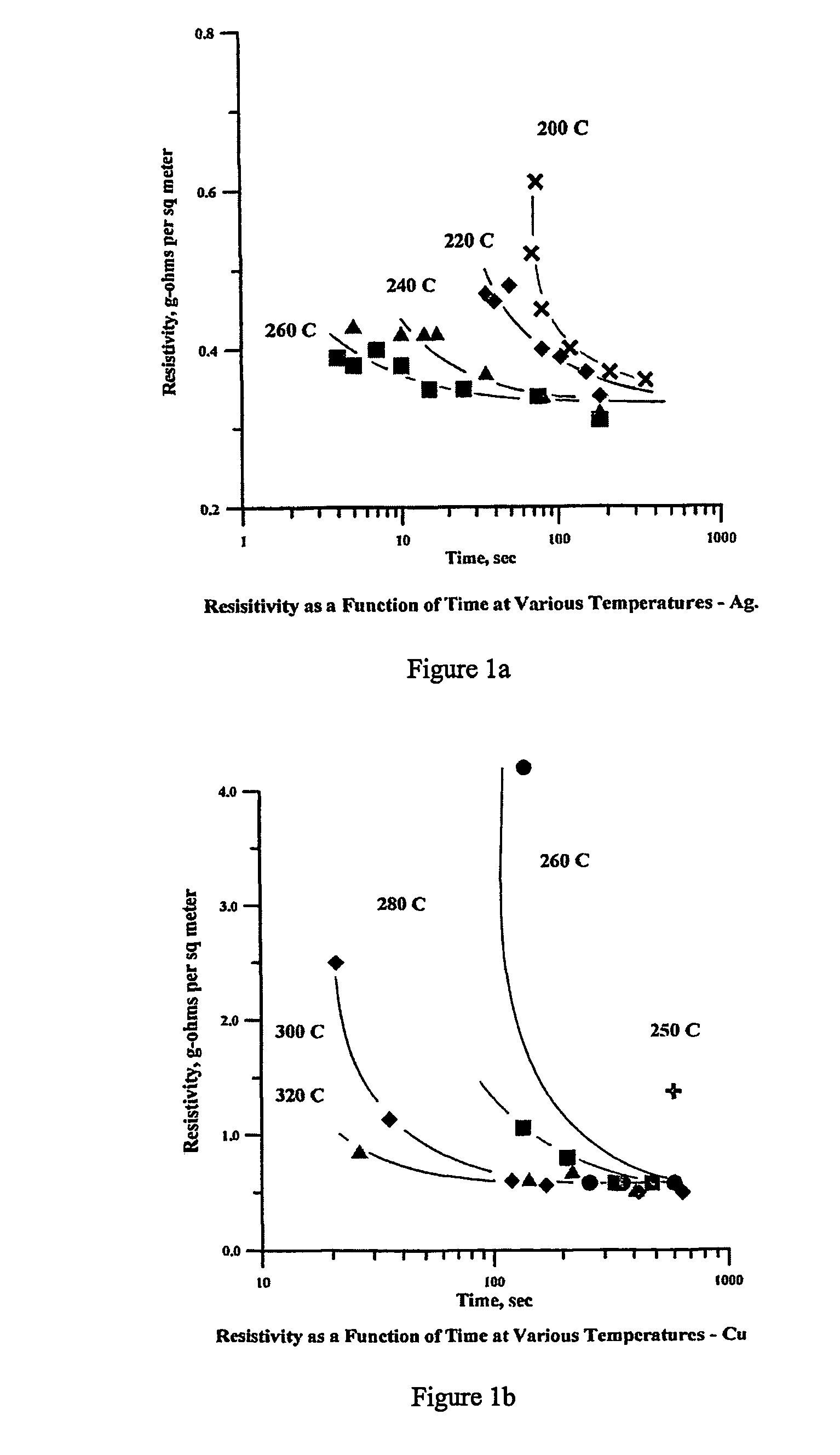
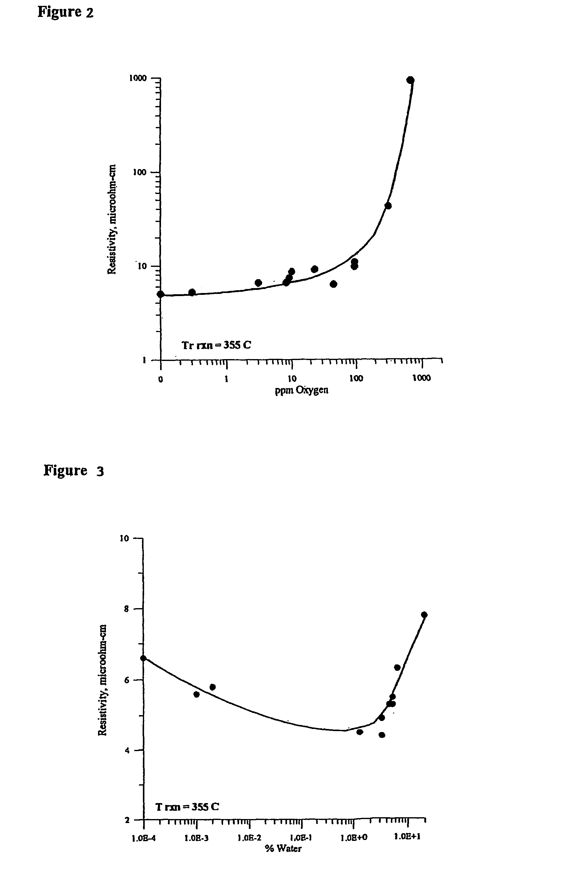
Image

Examples
example 1
[0121]A mixture of 52 parts by weight of −325 mesh spherical copper powder (Cerac C-1241, 30 parts by weight of 2–3 micrometer spherical copper powder (Cerac C-1229), 8 parts by weight colloidal copper powder with a mean diameter of approximately 0.1 micrometer made by reducing copper acetate in ethylene glycol with hydrazine hydrate (the well-known glycol synthesis), and 10 parts by weight neodecanoic acid (Exxon Chemical Prime Grade) was prepared. The mixture was combined and blended by hand in a nitrogen glove box. The mixture was roll milled in air to produce a homogeneous ink. The ink was screen printed onto a DuPont Kapton® ELJ dielectric substrate at room temperature in air. The traces were heat treated in a belt furnace at 330° C. for 6–10 minutes in the hot zone in a N2—H2O—H2 atmosphere.
[0122]After heating, the components were dry to the touch, the organic constituents having been completely removed. The electrical resistivity of the bright copper circuit trace measured by...
example 2
[0123]A mixture 72 parts by weight of 2–3 micrometer diameter spherical copper powder (Cerac C-1229, 16 parts by weight colloidal copper powder with a mean diameter of approximately 0.1 micrometer made by reducing copper acetate in ethylene glycol with hydrazine hydrate, and 12 parts by weight neodecanoic acid (Exxon Chemical Prime Grade) was prepared. The mixture was combined and blended by hand in a glove box. The mixture was roll milled in air to produce homogeneous ink. The ink was screen printed onto a DuPont Kapton® ELJ dielectric substrate at room temperature in air. The traces were heat treated in a belt furnace at 330° C. for 6–10 minutes in the hot zone in a N2—H2O—H2 atmosphere.
[0124]After heating, the components were dry to the touch, the organic constituents having been completely removed. The electrical resistivity of the bright copper circuit trace measured by IPC Test Method 2.5.13 was 0.47 g-ohms per m2. Scotch tape was applied to the circuit trace and immediately r...
example 3
[0125]A mixture 57 parts by weight of 0.5 micrometer diameter spherical copper powder (Canadian Electronic Powders Corp St. Laurent Quebec, Canada, Cu-0500), 23 parts by weight colloidal copper powder with a mean diameter of approximately 0.1 micrometers made by reducing copper acetate in ethylene glycol with hydrazine hydrate, and 20 parts by weight of neodecanoic acid (Exxon Chemical Prime Grade) was prepared. The mixture was combined and blended by hand in a glove box. The mixture was roll milled in air to produce a homogeneous ink. The ink was screen printed onto a DuPont Kapton® ELJ dielectric substrate at room temperature in air. The traces were heat treated in a belt furnace at 330° C. for 6–10 minutes in the hot zone in a N2—H2O—H2 atmosphere.
[0126]After heating, the components were dry to the touch, the organic constituents having been completely removed. The electrical resistivity of the bright copper circuit trace measured by IPC Test Method 2.5.13 was 0.47 g-ohms per m2....
PUM
 Abstract
Description
Claims
Application Information