Systems and methods of forming refractory metal nitride layers using disilazanes

a technology of refractory metal nitride and disilazanes, which is applied in the direction of coatings, chemical vapor deposition coatings, capacitors, etc., can solve the problems of frequent creation of undesirable interfacial layers of siosub>2 /sub>, high leakage paths and channels, and dielectric layers approaching only 10 in thickness, so as to minimize the effect of detrimental gas phase reactions and improved control of layer thickness

Inactive Publication Date: 2006-10-17
MICRON TECH INC
View PDF57 Cites 179 Cited by
  • Summary
  • Abstract
  • Description
  • Claims
  • Application Information

AI Technical Summary

Benefits of technology

[0021]“Barrier layer” as used herein refers to a conductive, interfacial layer that can reduce diffusion of ambient oxygen through a dielectric layer into a semiconductor substrate (typically a polysilicon substrate) or can reduce diffusion of one layer into another, such as a copper conductive layer into a semiconductor substrate (typically a polysilicon substrate). For this invention, the barrier layer is a tantalum nitride or tantalum silicon nitride layer.
[0026]“Atomic layer deposition” (ALD) as used herein refers to a vapor deposition process in which numerous consecutive deposition cycles are conducted in a deposition chamber. Typically, during each cycle the metal precursor is chemisorbed to the substrate surface; excess precursor is purged out; a subsequent precursor and / or reaction gas is introduced to react with the chemisorbed layer; and excess reaction gas (if used) and by-products are removed. As compared to the one cycle chemical vapor deposition (CVD) process, the longer duration multi-cycle ALD process allows for improved control of layer thickness by self-limiting layer growth and minimizing detrimental gas phase reactions by separation of the reaction components. The term “atomic layer deposition” as used herein is also meant to include the related terms “atomic layer epitaxy” (ALE) (see U.S. Pat. No. 5,256,244 (Ackerman)), molecular beam epitaxy (MBE), gas source MBE, organometallic MBE, and chemical beam epitaxy when performed with alternating pulses of precursor compound(s), reaction gas and purge (i.e., inert carrier) gas.

Problems solved by technology

However, the continuous shrinkage of microelectronic devices over the years has led to dielectric layers approaching only 10 Å in thickness (corresponding to 4 or 5 molecules).
However, these metal-containing layers can provide high leakage paths and channels for oxygen diffusion, especially during annealing.
Also, an undesirable interfacial layer of SiO2 is frequently created by oxidation of polysilicon during the annealing of the dielectric layer.
This copper diffusion has led to degradation of device reliability, causing semiconductor manufacturers to turn toward other less conductive metals, such as aluminum and tungsten.
However, when PVD methods are used, the stoichiometric composition of the formed metal nitride and metal silicon nitride barrier layers such as Ta—N and Ta—Si—N can be non-uniform across the substrate surface due to different sputter yields of Ta, Si, and N. Due to the resulting poor layer conformality, defects such as pinholes often occur in such layers creating pathways to diffusion.

Method used


Image

  • Systems and methods of forming refractory metal nitride layers using disilazanes
  • Systems and methods of forming refractory metal nitride layers using disilazanes
  • Systems and methods of forming refractory metal nitride layers using disilazanes

Examples


example 1

Pulsed Chemical Vapor Deposition of Tantalum Silicon Nitride

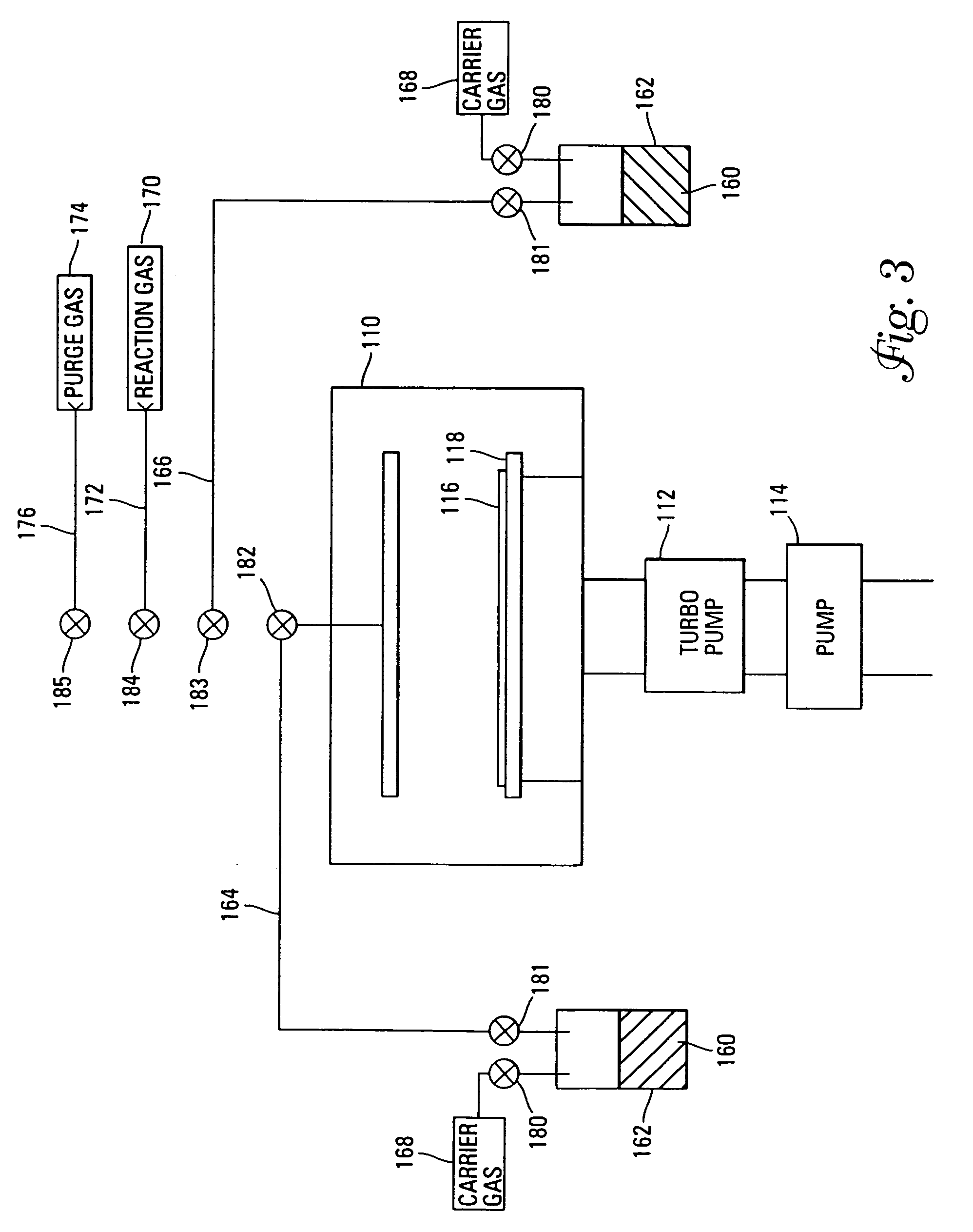
[0072]Using a pulsed CVD method, the following precursor compounds were pulsed for 200 cycles in a deposition chamber as described in FIG. 3 containing a borophosphosilicate glass (BPSG) substrate, each cycle consisting of pulses in the following order: (1) tantalum pentafluoride (Alfa Aesar, Ward Hill, Mass.), (2) tetramethyldisilazane (TMDS) (Sigma-Aldrich Chemical C., Milwaukee, Wis.), (3) tantalum pentafluoride and (4) disilane (VOC Gases). During each cycle, excess amounts of each precursor compound not chemisorbed were purged from the chamber after chemisorption and prior to the introduction of the next precursor compound using an argon sweep at 30 mL / min and a vacuum pump. The substrate temperature was kept at approximately 320° C. throughout the entire deposition process.

[0073]At the end of the pulsed CVD process, a 1375 Å thick mirror-like layer of tantalum silicon nitride was formed. The layer contained about 54 a...


PUM

PropertyMeasurementUnit
temperatureaaaaaaaaaa
pressureaaaaaaaaaa
temperatureaaaaaaaaaa

Abstract

A method of forming (and apparatus for forming) refractory metal nitride layers (including silicon nitride layers), such as a tantalum (silicon) nitride barrier layer, on a substrate by using a vapor deposition process with a refractory metal precursor compound, a disilazane, and an optional silicon precursor compound.

Description

[0001]This is a divisional of application Ser. No. 10 / 229,802, filed Aug. 28, 2002, now U.S. Pat No. 6,794,284, which is incorporated herein by reference.FIELD OF THE INVENTION[0002]This invention relates to methods of forming refractory metal nitride layers (including silicon nitride layers) on substrates using a vapor deposition process with a refractory metal halide (preferably, fluoride) precursor compound, a disilazane, and optionally a silicon precursor compound. The formed refractory metal (silicon) nitride layers are particularly useful as diffusion barriers for polysilicon substrates to reduce diffusion of oxygen, copper, or silicon.BACKGROUND OF THE INVENTION[0003]In integrated circuit manufacturing, microelectronic devices such as capacitors are the basic energy storage devices in random access memory devices, such as dynamic random access memory (DRAM) devices, static random access memory (SRAM) devices, and ferroelectric memory (FERAM) devices. Capacitors typically cons...

Claims


Application Information

Patent Timeline
Patent Type & Authority Patents(United States)
IPC IPC(8): H01L21/4763C23C16/34H01L21/285H01L21/768
CPCC23C16/34C23C16/45523C23C16/45531C23C16/45553H01L21/28556H01L21/28562H01L21/76841H01L21/76864H01L28/60H01L28/55
Inventor VAARTSTRA, BRIAN A.
Owner MICRON TECH INC
Why Eureka
Try Eureka