High-aspect ratio anode and apparatus for high-speed electroplating on a solar cell substrate

a solar cell substrate and high-aspect ratio technology, applied in the direction of vacuum evaporation coating, optical elements, coatings, etc., can solve the problems of greater resistive loss, loss of efficiency, and discontinuous formation of conductor thin fingers, when formed by screen printing process

Inactive Publication Date: 2010-04-27
APPLIED MATERIALS INC
View PDF63 Cites 29 Cited by
  • Summary
  • Abstract
  • Description
  • Claims
  • Application Information

AI Technical Summary

Benefits of technology

[0024]Embodiments of the present invention may further provide a method of forming a metal layer on a solar cell substrate, comprising disposing a first surface of a masking plate over at least a portion of a seed layer formed on a substrate, wherein the masking plate has a plurality of apertures that are in communication with a first surface of the masking plate, contacting the seed layer formed on the substrate with one or more electrical contacts, forming a first metal layer over the seed layer formed on the substrate by immersing the substrate and a first electrode in an electrolyte and biasing the one or more electrical contacts relative to the first electrode using one or more power supplies, wherein the first metal layer is simultaneously formed on the substrate within the areas exposed by apertures formed in the first masking plate, and biasing a second electrode that is disposed in the electrolyte relative to the one or more electrical contacts or the first electrode while forming the first metal layer to vary the uniformity of the deposited first metal layer. In one embodiment, a method can be used to plate between 2 and 1000 substrates at a time.

Problems solved by technology

Further, resistive losses experienced by a PUM connected device will not increase as the solar cell surface area increases and, hence, larger solar cells may be manufactured without a loss in efficiency.
However, there are several issues with this manufacturing method.
First, the thin fingers of the conductors, when formed by the screen printing process, may be discontinuous since the fingers formed using a metal paste do not always agglomerate into a continuous interconnecting line during the annealing process.
Second, porosity present in the fingers formed during the agglomeration process results in greater resistive losses.
Shunts on the substrate backside are caused by poor definition of backside contacts such as waviness, and / or metal residue.
Fourth, due to the relatively thin substrate thicknesses commonly used in solar cell applications, such as 200 micrometers and less, the act of screen printing the metal paste on the substrate surface can cause physical damage to the substrate.
Lastly, silver-based paste is a relatively expensive material for forming conductive components of a solar cell.
One issue with the current method of forming metal interconnects using a screen printing process that utilizes a metal particle containing paste is that the process of forming the patterned features requires high temperature post-processing steps to densify the formed features and form a good electrical contact with the substrate surface.
A high extrinsic stress, or even intrinsic stress, formed in the metal interconnect lines is an issue, since it can cause breakage of the formed metallized features, warping of the thin solar cell substrate, and / or delamination of the metallized features from the surface of the solar cell substrate.
The high temperature post processing step can also cause the material in the solar cell device to diffuse into unwanted regions of the device, thus causing device problems, such as an electrical short.
High temperature processes also limit the types of materials that can be used to form a solar cell due to the breakdown of certain materials at the high sintering temperatures.
Also, screen printing processes also tend to be non-uniform, unreliable and often unrepeatable.
However the laser-cut grooves are a source of macro- and micro-defects.
The laser-cut edge is not well defined, causing waviness on the finger edges, and the heat of the laser introduces defects into the silicon.
If the substrate throughput is not limited by the time to transfer the solar cell substrates then the longest process recipe step will generally limit the throughput of the processing sequence, increase the CoO and possibly make a desirable processing sequence impractical.

Method used


Image

  • High-aspect ratio anode and apparatus for high-speed electroplating on a solar cell substrate
  • High-aspect ratio anode and apparatus for high-speed electroplating on a solar cell substrate
  • High-aspect ratio anode and apparatus for high-speed electroplating on a solar cell substrate

Examples


example 1

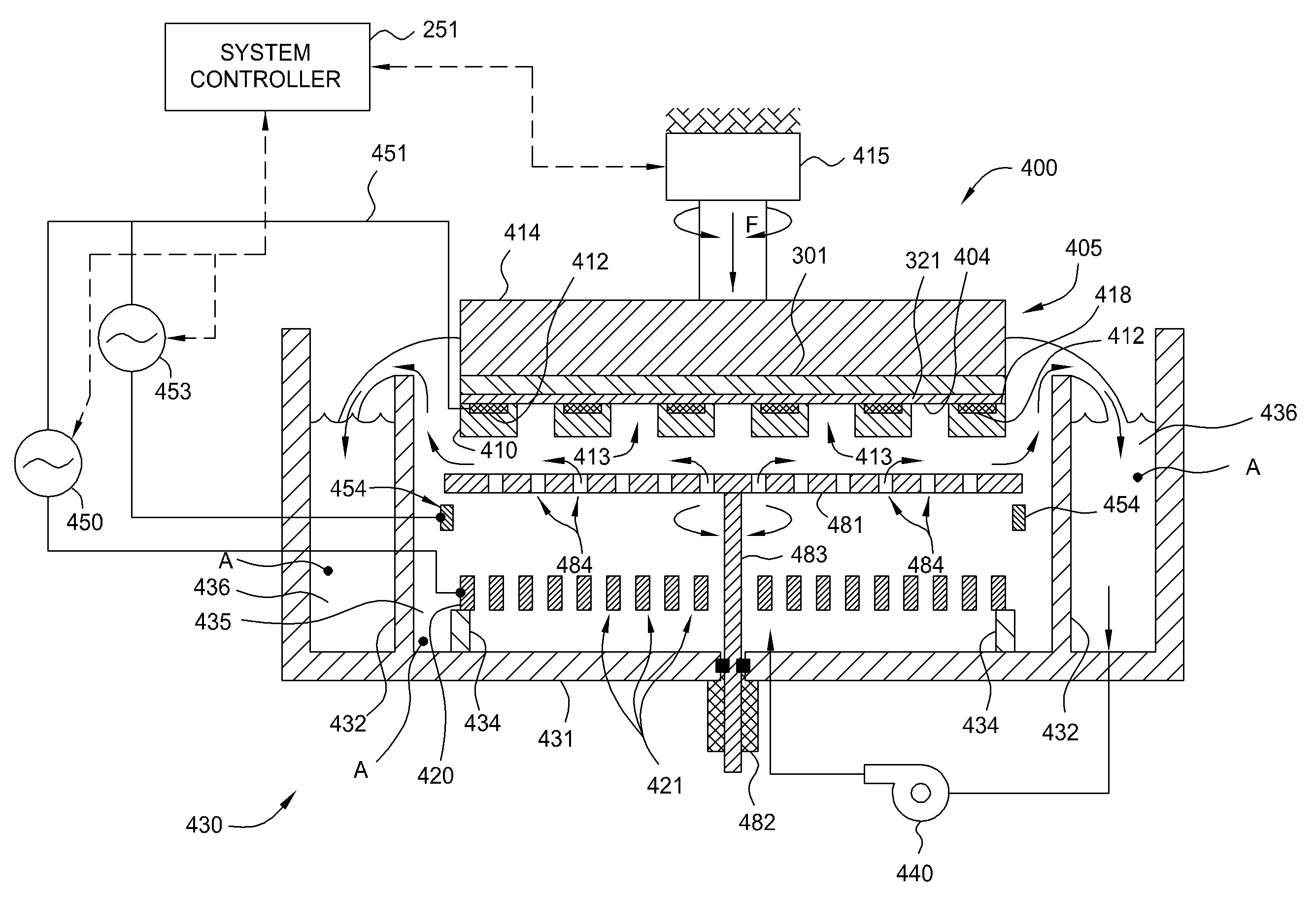
[0081]In one example, the electrolyte is an aqueous solution that contains between about 200 and 250 g / l of copper sulfate pentahydrate (CuSO4.5(H2O)), between about 40 and about 70 g / l of sulfuric acid (H2SO4), and about 0.04 g / l of hydrochloric acid (HCl). In some cases it is desirable to add a low cost pH adjusting agent, such as potassium hydroxide (KOH) or sodium hydroxide (NaOH) to form an inexpensive electrolyte that has a desirable pH to reduce the cost of ownership required to form a metal contact structure for a solar cell. In some cases it is desirable to use tetramethylammonium hydroxide (TMAH) to adjust the pH. Could go to high copper concentration with organic complexing agent to solution, such as MSA. In one aspect, a low acid chemistry is used to complete the high speed deposition process. An example of some exemplary copper plating chemistries that may be used for high speed plating is further described in commonly assigned U.S. Pat. Nos. 6,113,771, 6,610,191, 6,350...

example 2

[0082]In another example, the electrolyte is an aqueous solution that contains between about 220 and 250 g / l of copper fluoroborate (Cu(BF4)2), between about 2 and about 15 g / l of tetrafluoroboric acid (HBF4), and about 15 and about 16 g / l of boric acid (H3BO3). In some cases it is desirable to add a pH adjusting agent, such as potassium hydroxide (KOH), or sodium hydroxide (NaOH) to form an inexpensive electrolyte that has a desirable pH to reduce the cost of ownership required to form a metal contact structure for a solar cell. In some cases it is desirable to use tetramethylammonium hydroxide (TMAH) to adjust the pH.

example 3

[0083]In yet another example, the electrolyte is an aqueous solution that contains between about 60 and about 90 g / l of copper sulfate pentahydrate (CuSO4.5(H2O)), between about 300 and about 330 g / l of potassium pyrophosphate (K4P2O7), and about 10 to about 35 g / l of 5-sulfosalicylic acid dehydrate sodium salt (C7H5O6SNa.2H2O). In some cases it is desirable to add a pH adjusting agent, such as potassium hydroxide (KOH), or sodium hydroxide (NaOH) to form an inexpensive electrolyte that has a desirable pH to reduce the cost of ownership required to form a metal contact structure for a solar cell. In some cases it is desirable to use tetramethylammonium hydroxide (TMAH) to adjust the pH.


PUM

PropertyMeasurementUnit
thicknessesaaaaaaaaaa
thicknessaaaaaaaaaa
thicknessaaaaaaaaaa

Abstract

Embodiments of the invention contemplate the formation of a low cost solar cell using a novel high speed electroplating method and apparatus to form a metal contact structure having selectively formed metal lines using an electrochemical plating process. The apparatus and methods described herein remove the need to perform one or more high temperature screen printing processes to form conductive features on the surface of a solar cell substrate. The resistance of interconnects formed in a solar cell device greatly affects the efficiency of the solar cell. It is thus desirable to form a solar cell device that has a low resistance connection that is reliable and cost effective. Therefore, one or more embodiments of the invention described herein are adapted to form a low cost and reliable interconnecting layer using an electrochemical plating process containing a common metal, such as copper.

Description

CROSS-REFERENCE TO RELATED APPLICATIONS[0001]This application is related to the U.S. patent application Ser. No. 11 / 566,205 entitled “Precision Printing Electroplating Through Plating Mask On A Solar Cell Substrate” by Sergey Lopatin et al., filed Dec. 1, 2006, the U.S. patent application Ser. No. 11 / 566,201 entitled “Method Of Metallizing A Solar Cell Substrate” by Sergey Lopatin et al., filed Dec. 1, 2006, and the U.S. patent application Ser. No. 11 / 566,205 entitled “Electroplating On Roll-to-Roll Flexible Solar Cell Substrates” by Sergey Lopatin et al., filed Dec. 1, 2006, which are all herein incorporated by reference.BACKGROUND OF THE INVENTION[0002]1. Field of the Invention[0003]Embodiments of the present invention generally relate to the fabrication of photovoltaic cells.[0004]2. Description of the Related Art[0005]Solar cells are photovoltaic devices that convert sunlight directly into electrical power. The most common solar cell material is silicon, which is in the form of ...

Claims


Application Information

Patent Timeline
Patent Type & Authority Patents(United States)
IPC IPC(8): C25D17/00
CPCC25D5/022C25D7/08C25D17/00C25D17/001H01L31/022433C25D17/008H01L31/022425Y02E10/50
Inventor LOPATIN, SERGEYKOVARSKY, NICOLAY Y.EAGLESHAM, DAVIDDUKOVIC, JOHN O.GAY, CHARLES
Owner APPLIED MATERIALS INC
Why Eureka
Try Eureka