Method of manufacturing a flexible circuit electrode array

Active Publication Date: 2011-03-29
CORTIGENT INC
View PDF20 Cites 111 Cited by
  • Summary
  • Abstract
  • Description
  • Claims
  • Application Information

AI Technical Summary

Benefits of technology

[0033]The present invention provides a flexible circuit electrode array with excellent adhesion and insulating properties of a polymer insulator reached by a new technique of activation of a base polymer layer prior to applying a top polymer layer wherein both polymer layers result in one polymer layer. The adhesion and insulating properties are further improved by applying a top metal layer

Problems solved by technology

However, encapsulation proves difficult to effectively implement with this method.
Gold, while biocompatible, is not completely stable under the c

Method used


Image

  • Method of manufacturing a flexible circuit electrode array
  • Method of manufacturing a flexible circuit electrode array
  • Method of manufacturing a flexible circuit electrode array

Examples


Example

EXAMPLE 1

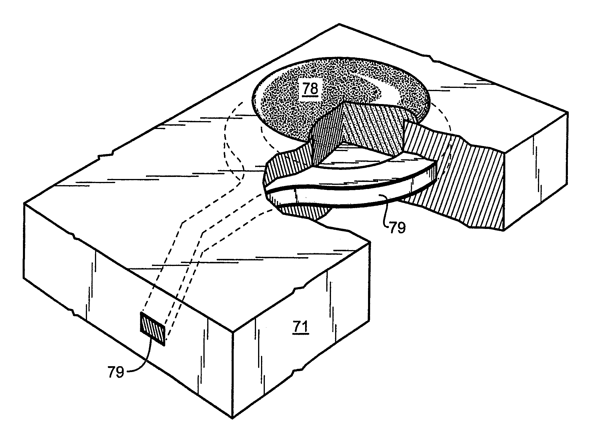
[0121]A 10.2 cm×10.2 cm×0.15 cm supporting glass plate substrate 70 was marked with a batch and plate identification code by mechanical engraving. Then a 5.5 μm thick layer of polyimide BPDA / PDA (derived from 3,3′,4,4′-biphenyltetracarboxylic dianhydride (BPDA) and p-phenylendiamine (PDA)) layer 71a was applied onto the front side of the glass plate 70 as a liquid precursor by spin coating and cured to Polyimide, PI2611.

[0122]Then a 0.05 μm layer of titanium 72a was applied on the polyimide layer 71a preferably by magnetron sputtering, a 0.5 μm layer of platinum 73 was applied on the titanium layer 72a preferably by magnetron sputtering, and a 0.10 μm layer of titanium 72b was applied onto the layer of platinum 73 preferably by magnetron sputtering yielding a titanium / platinum / titanium thin film stack.

[0123]Subsequently a 2 μm layer 74 of positive photoresist AZ 1512 (Microchemicals GmbH, Germany) was applied on the titanium layer 72b. The photoresist layer 74 was irradiate...

Example

[0135]Example 2 was carried out according to example 1 with the difference that the base polyimide surface layer 71a was activated and partially removed by RIE in all areas not covered by trace metal conductors. The surface was treated in 100 mTorr, 85% O2, 15% CF4 for 2 min at 200 W and 20° C. as shown in the preceding table 1 and the deimidization was omitted. The adhesion strength between the base polyimide layer 71a and the top polyimide layer 71b is shown in table 3.

[0136]TABLE 3Adhesion StrengthPolyimide - PolyimideAdhesion Polyimide - PolyimideStrength [N]Adhesion Strength [N]ExRIEDeimidizationDryWet185% O2,3.02.415% CF4

[0137]Table 3 shows the measurement of two adhered dry polyimide films and two adhered polyimide films kept in saline solution for 7 days at 87° C.

Example

[0138]Example 3 was carried out according to example 1 with the difference that the base polyimide surface layer 71a was activated by deimidization. The surface was subsequently treated in KOH-deimidization bath at 25° C. for 5 min with manual agitation of the carrier boat at least every 60 s. The surface was first rinsed in a lower cascade rinse bath for 60 s, in a middle cascade rinse bath for 60 s, and finally in a bubbler cascade rinse bath for 60 s. The surface was dried with filtered nitrogen. The surface was then treated in an HCl-deimidization bath at 25° C. for 5 min with manual agitation of the carrier boat at least every 60 s. The surface was first rinsed in a lower cascade rinse bath for 60 s, in a middle cascade rinse bath for 60 s, and finally in a bubbler cascade rinse bath for 60 s. The deimidization process is shown in the following table 2 and the RIE was omitted. The adhesion strength between the base polyimide layer 71a and the top polyimide layer 71b is shown in...


PUM


Abstract

Polymer materials form electrode array bodies for neural stimulation, especially for retinal stimulation to create vision. The method lays down a polymer layer. Apply a metal layer to the polymer and pattern to create electrodes and leads. Apply a second polymer layer over the metal layer and pattern to leave openings for electrodes. The array and its supply cable are a single body. A method for manufacturing a flexible circuit electrode array, is: deposit a metal trace layer on an insulator polymer base layer; apply a layer of photoresist on the metal trace layer and pattern the metal trace layer and form metal traces on the insulator polymer base layer; activate the insulator polymer base layer and deposit a top insulator polymer layer and form a single insulating polymer layer with the base insulator polymer layer; wherein the insulator polymer layers are heated at 80-150° C. and then at 230-350° C.

Description

CROSS-REFERENCE TO RELATED APPLICATIONS[0001]This application claims priority of U.S. Application No. 60 / 772,099, “Flexible Circuit Electrode Array and Method of Manufacturing the Same,” filed Feb. 10, 2006, the disclosure of which is incorporated herein by reference.STATEMENT REGARDING FEDERALLY SPONSORED RESEARCH OR DEVELOPMENT[0002]This invention was made with government support under grant No. R24EY12893-01, which has been awarded by the National Institutes of Health. The government has certain rights in the invention.BACKGROUND OF THE INVENTION[0003]1. Field of the Invention[0004]The present invention is generally directed to a flexible circuit electrode array especially for biomedical implants, especially implantable medical devices, such as retinal prosthesis and a method of manufacturing the flexible circuit electrode array.[0005]2. Description of the Related Art[0006]In U.S. Pat. No. 3,699,970 “Striate Cortex Stimulator” to Giles Skey Brindley et al. an implantable device i...

Claims


Application Information

Patent Timeline
IPC IPC(8): A61N1/04
CPCA61N1/0543H05K3/0011H05K3/0035H05K3/064H05K2203/0736H05K2203/095
Inventor GREENBERG, ROBERT J.TALBOT, NEIL HAMILTONNEYSMITH, JORDAN MATTHEWOK, JERRYMECH, BRIAN V.
Owner CORTIGENT INC
Why Eureka
Try Eureka