Eureka AIR delivers breakthrough ideas for toughest innovation challenges, trusted by R&D personnel around the world.

Methods and materials for making a monolithic porous pad cast onto a rotatable base

a monolithic porous pad and rotatable base technology, applied in the direction of metal-working apparatus, floor surfacing/polishing machines, tableware washing/rinsing machines, etc., can solve the problems of reliability and functional problems in the integrated circuit, the presence of trace metals, mobile ions on wafers, and the presence of particulate contamination, etc., to reduce localized non-uniform flushing of the porous pad, increase the overall amount of liquid used, reduce the effect of localized

Active Publication Date: 2011-07-26
ENTEGRIS INC
View PDF29 Cites 10 Cited by
  • Summary
  • Abstract
  • Description
  • Claims
  • Application Information

AI Technical Summary

Benefits of technology

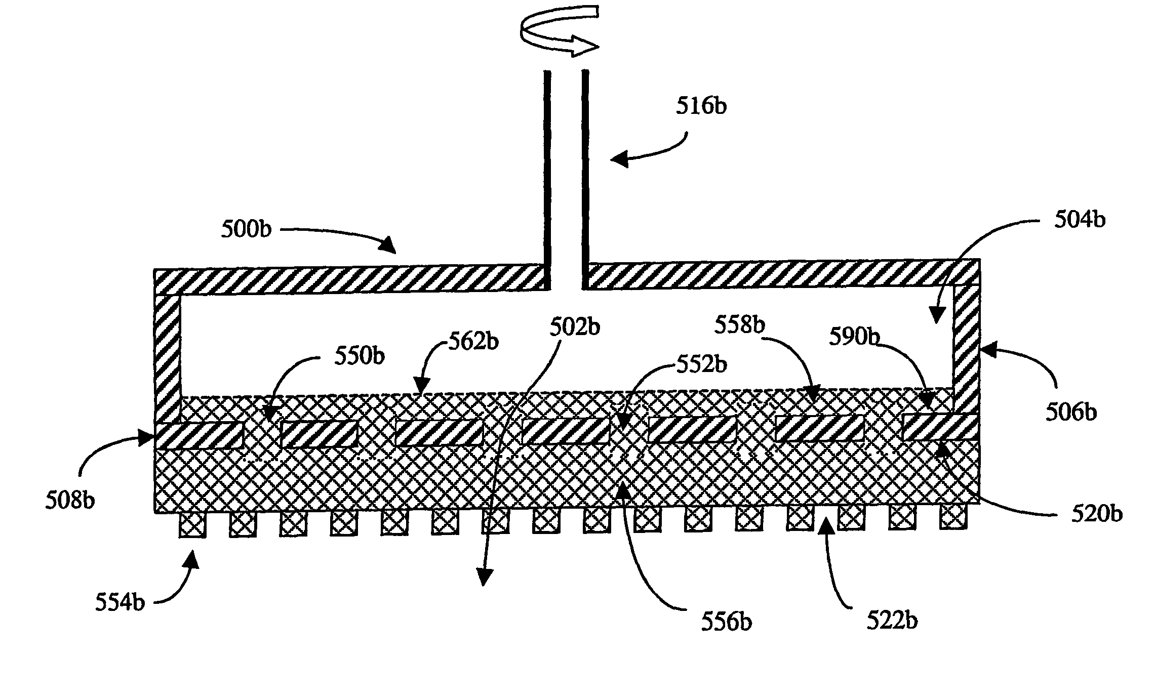
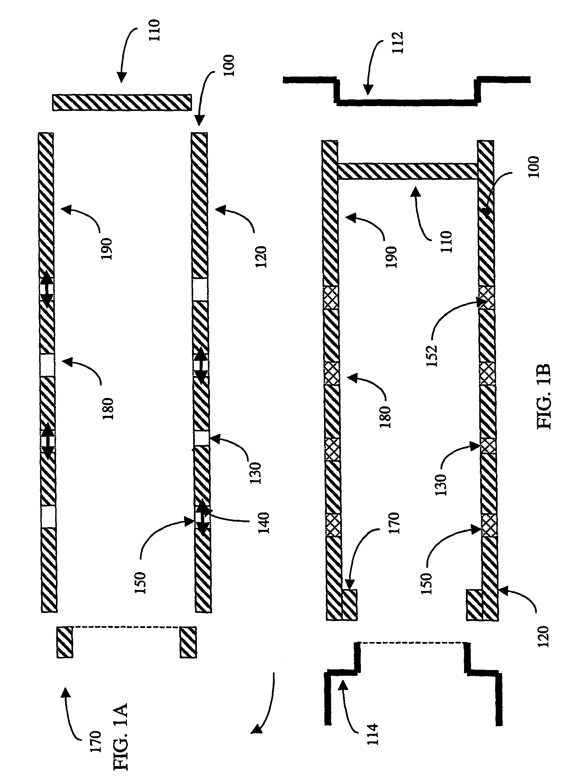
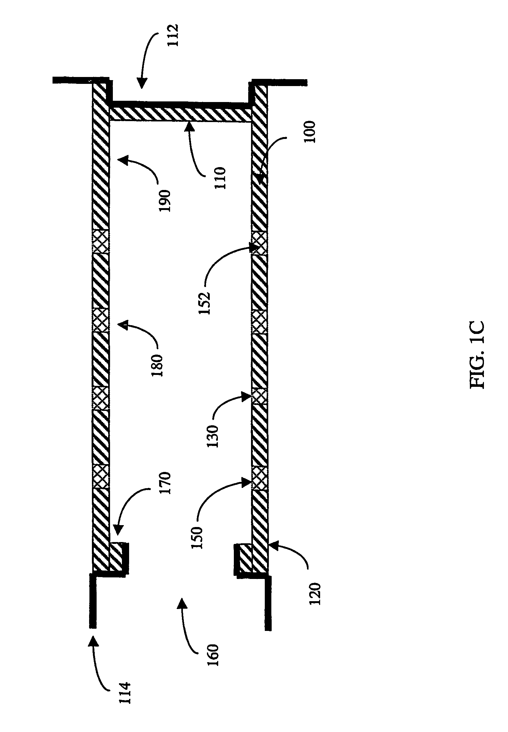
Advantageously, embodiments of the present invention may be used to provide a fluid to the surface of a substrate for a cleaning or material removal operation such as a chemical mechanical planarization or post CMP scrubbing processes. By interlocking the porous pad material with the base, the porous pad material in held in place relative to the base. Node misalignment and twisting in embodiments of the present invention substantially reduces or eliminated brush walking and twisting compared to slip on sleeve style brushes. An additional advantage of the present invention is that it may be used to distribute fluid to both roller and pad type base fixtures. The porous pad material in the channels may also be used to control the liquid flow from the fluid source to the substrate. This allows the number of perforations or through channels in the housing core to be decreased and their size or surface area increased without significantly increasing the overall amount of liquid used. This is particularly advantageous since larger perforations or through channels in the housing reduces localized nonuniform flushing of the porous pad. Further, by restricting the flow of liquid, the porous pad causes a uniform pressure buildup inside of the distributor. This in turn can be used to form through holes that ensure that both ends of the brush receive the same amount of liquid and are uniformly flushed which improves particulate removal from the brush and reduces or eliminates uneven wear of the brush.
is that it may be used to distribute fluid to both roller and pad type base fixtures. The porous pad material in the channels may also be used to control the liquid flow from the fluid source to the substrate. This allows the number of perforations or through channels in the housing core to be decreased and their size or surface area increased without significantly increasing the overall amount of liquid used. This is particularly advantageous since larger perforations or through channels in the housing reduces localized nonuniform flushing of the porous pad. Further, by restricting the flow of liquid, the porous pad causes a uniform pressure buildup inside of the distributor. This in turn can be used to form through holes that ensure that both ends of the brush receive the same amount of liquid and are uniformly flushed which improves particulate removal from the brush and reduces or eliminates uneven wear of the brush.
An advantage of a brush cast onto a disposable core is that the core and brush are joined together eliminating the slippage, expansion, and loss of concentricity observed with brushes friction fit onto a core. The brush cast onto the core eliminates the need for special mounting stand and time associated with mounting friction brush sleeves onto cores.

Problems solved by technology

Without planarization, fabrication of further interconnect and dielectric layers becomes substantially more difficult due to the higher variations in the surface topography.
In the manufacture of electronic devices such as integrated circuits, the presence of particulate contamination, trace metals, and mobile ions on a wafer is a serious problem.
Particulate contamination can cause a wide variety of problems such as localized corrosion, scratching, and “shorts” in the integrated circuit.
Mobile ion and trace metal contaminants can also lead to reliability and functional problems in the integrated circuit.
The combination of these factors results in lower device yields on a wafer, thereby increasing the cost of an average functional device on the wafer.
After extended use, the brush is replaced with a new brush sleeve and requires the polishing tool be stopped adding to lost productivity and downtime.
Asymmetric alignment and distortion of the spacing of the nodes on the sleeve is a problem with sleeve replacement.
This non-value added step is costly for manufactures in time and dummy wafers.
As semiconductor feature sizes decrease and device performance requirements continue increase, cleaning engineers are also challenged to improve their associated processes.
Many cleaning systems are now required to also apply reactive chemicals, such as hydrofluoric acid, uneven application will have a severe impact on the wafer being processed.

Method used


Image

  • Methods and materials for making a monolithic porous pad cast onto a rotatable base
  • Methods and materials for making a monolithic porous pad cast onto a rotatable base
  • Methods and materials for making a monolithic porous pad cast onto a rotatable base

Examples


example 1

A quantity of Airvol V-107 was purchased from Air Products Inc. The polyvinylalcohol was dissolved as follows: 180 g polyvinylalcohol V-107 and 600 grams of tap water. The mixture was mixed and heated to about 100° C. until all the polyvinyl alcohol dissolved.

From this mixture, small test batches were made as follows: 175 grams. polyvinylalcohol solution 30%; 48 grams formaldehyde 37%; 27 grams sulfuric acid 36%; and 13.5 grams corn starch. These ingredients were mixed in the order starch, H2SO4, formaldehyde, and last the 30% PVA solution. This new mixture was free of entrained air. The solution was of low viscosity, opaque, and at room temperature. All of this material was poured into a polyvinylchloride mold and heated to 70° C. for three hours. Inspection of the sponge formed in the mold revealed excess bonding to the PVC mold surface. Some sponge material was treated with H2O2 / NaHCO3 and investigated.

The sponge was well developed, white, soft, and conformed well to the mold wit...

example 2

Another part of this invention is a method for preparing a PVC brush mold so that the inventive cleaning brush can be removed efficiently the mold without tearing the bristles from the exterior surface of the brush. It has been found that prior to injecting a PVC brush mold with PVA, that applying a preferred mixture of tetrahydrofuran (THF) and paraffin to the PVC mold creates a coating on which PVA does not appreciably stick. Upon completion of manufacturing, using a PVC mold prepared by the method described, the brush can be easily removed from the mold by hand.

Without wishing to be bound by theory, the paraffin and THF mixture, when applied in proper proportions is believed to act upon the PVC material by forming an alloy layer comprised of some or all of the elements PVC, THF, and paraffin. This alloy layer is in the form of a visible sheen which can be physically scratched off of the mold until the pure PVC located below the alloy layer, is exposed. The alloy layer is durable ...

example 3

This prophetic example describes cleaning a wafer having a layer of copper metal following a chemical mechanical planarization process. The wafer may be introduced into a first brush box of the cleaning system. In the first brush box cleaning chemical can be applied to the wafer through the brushes which are formed of a cast on core porous pad material interlocking to the base core of the brush. The cleaning chemical applied through the brushes in the first brush box controllably transforms copper material on the substrate surface into a water soluble form. The copper material is transformed into a water soluble form in order to remove a controlled amount of copper from the surface of the wafer. The wafer can be moved from the first brush box to the second brush box. In the second brush box a second cleaning chemical may be applied to the surface of the wafer through the brushes of the second brush box in order to clean the wafer surface and clean the brushes of copper. The second c...


PUM

PropertyMeasurementUnit
diameteraaaaaaaaaa
thicknessaaaaaaaaaa
thicknessaaaaaaaaaa

Abstract

The present invention includes methods and materials for making a brush or pad for removing materials, particles, or chemicals from a substrate. The brush or pad includes a rotatable base for supporting a porous pad material. The base include an inner surface and an outer surface and a plurality of channels in the base for interlocking the porous pad material with the base. A porous pad material covers at least a portion of the outer surface of the base and is used for removing material from various substrates. The porous pad material fills one or more of the channels in the base and interlocks the porous pad material with the base. Preferably the channels fluidly connect said inner surface with the outer surface of the base and aid in the alignment of porous pad nodes and the distribution of fluid within the porous pad.

Description

BACKGROUNDIn the fabrication of semiconductor devices, there is a need to perform chemical mechanical polishing (CMP) operations and wafer cleaning. Typically, integrated circuit devices are in the form of multi-level structures. At the wafer level, transistor devices having diffusion regions are formed. In subsequent levels, metal interconnect lines are patterned and electrically connected to the transistor devices to define the desired functional device. As is well known, patterned conductive layers are insulated from other conductive layers by dielectric materials, such as silicon dioxide. As more metallization levels and associated dielectric layers are formed, the need to planarize the dielectric material grows. Without planarization, fabrication of further interconnect and dielectric layers becomes substantially more difficult due to the higher variations in the surface topography. In semiconductor manufacturing processes, metal interconnect patterns are formed in a dielectric...

Claims


Application Information

Patent Timeline
Patent Type & Authority Patents(United States)
IPC IPC(8): B24B7/30B24D11/00B24D3/32B24D5/10
CPCB24D3/32A46B13/008B08B1/04A46B13/02H01L21/02074B24D5/10Y10S438/906A46B2200/3086Y10S134/902H01L21/67046B29K2029/04B08B1/34B24D5/00B29C44/1214B29C37/0078B29C44/005B29C44/1209B08B1/32B29C44/12
Inventor BENSON, BRIANT ENOCH
Owner ENTEGRIS INC
Why Eureka
Eureka Blog
Learn More