Semiconductor device manufacturing method and semiconductor device

a semiconductor and manufacturing method technology, applied in the direction of semiconductor devices, basic electric elements, electrical appliances, etc., can solve the problems of increasing the affecting the production efficiency so as to reduce the amount of warping and the effect of on resistance value of the back surface electrode formed

Inactive Publication Date: 2013-01-15
RENESAS ELECTRONICS CORP
View PDF11 Cites 0 Cited by
  • Summary
  • Abstract
  • Description
  • Claims
  • Application Information

AI Technical Summary

Benefits of technology

[0016]In Japanese Unexamined Patent Publication No. 2007-19458, A1 is sputtered to the surface of the silicon substrate which is polished at the back surface by an energy of 3 kW or higher as means for providing a semiconductor device without reducing the thickness of the silicon substrate and not conducting the annealing step (heat treatment). Then, the back surface electrode 310 is formed by re-crystallizing the amorphous silicon layer. Thus, the heat treatment after forming the back surface electrode 310 is saved. However, since the thickness of the amorphous silicon layer formed by the polishing of the back surface is not uniform, the contact resistance value of the silicon / Al contact portion formed by Al sputtering becomes not uniform. This results in unevenness of the on resistance. Accordingly, since the uniformness of electric properties in the wafer surface is worsened, this lowers the yield.
[0020]According to the present invention, since the single silicon crystal surface of the P type impurity diffusion layer is exposed by wet etching the P type impurity diffusion layer formed on the back surface of the silicon substrate, and forming the metal layer having a work function of 4.5 eV or more thereon at a temperature of the silicon substrate of 120° C. or lower, an ohmic contact between the P type impurity diffusion layer and the back surface electrode can be obtained without conducting the heat treatment after depositing the metal layers constituting the back surface electrode as in Japanese Patent No. 3,339,552 and Japanese Unexamined Patent Publication No. 2005-303218. Different from the patterned surface electrode, the back surface electrode is formed over the entire back surface of the silicon substrate. Therefore, while large warping is caused upon shrinkage by the heat treatment, since the temperature of the silicon substrate is set to 120° C. or lower upon forming the back surface electrode in the present invention, the problem of warping accompanying the shrinkage of the back surface electrode can be improved. Further, since the surface of the back surface electrode at least in contact with the P type impurity diffusion layer is provided with a metal layer having a work function of 4.5 eV or more, this forms a junction surface where the single silicon crystal surface and the metal layer having a work function of 4.5 eV or more are in contact with each other thereby capable of favorably keeping the resistance value of the ohmic contact.
[0021]The present invention provides an excellent effect capable of providing a semiconductor device that can reduce the amount of warping and the on resistance value of the back surface electrode formed on the back surface of the silicon substrate, as well as a manufacturing method thereof.

Problems solved by technology

However, according to the inventor's investigation, it has been found that the technique disclosed in the Patent documents described above involves problems to be improved.
The warping in the silicon substrate gives a trouble to the wafer transportation in the subsequent wafer probing and assembling steps.
As the size of the silicon substrate increases, warping of the silicon substrate gives more significant problem.
Therefore, it also involves a problem of generating warping in the silicon substrate in the same manner as in Japanese Patent No. 3,339,552.
However, since the thickness of the amorphous silicon layer formed by the polishing of the back surface is not uniform, the contact resistance value of the silicon / Al contact portion formed by Al sputtering becomes not uniform.
This results in unevenness of the on resistance.
Accordingly, since the uniformness of electric properties in the wafer surface is worsened, this lowers the yield.

Method used


Image

  • Semiconductor device manufacturing method and semiconductor device
  • Semiconductor device manufacturing method and semiconductor device
  • Semiconductor device manufacturing method and semiconductor device

Examples


embodiment 1

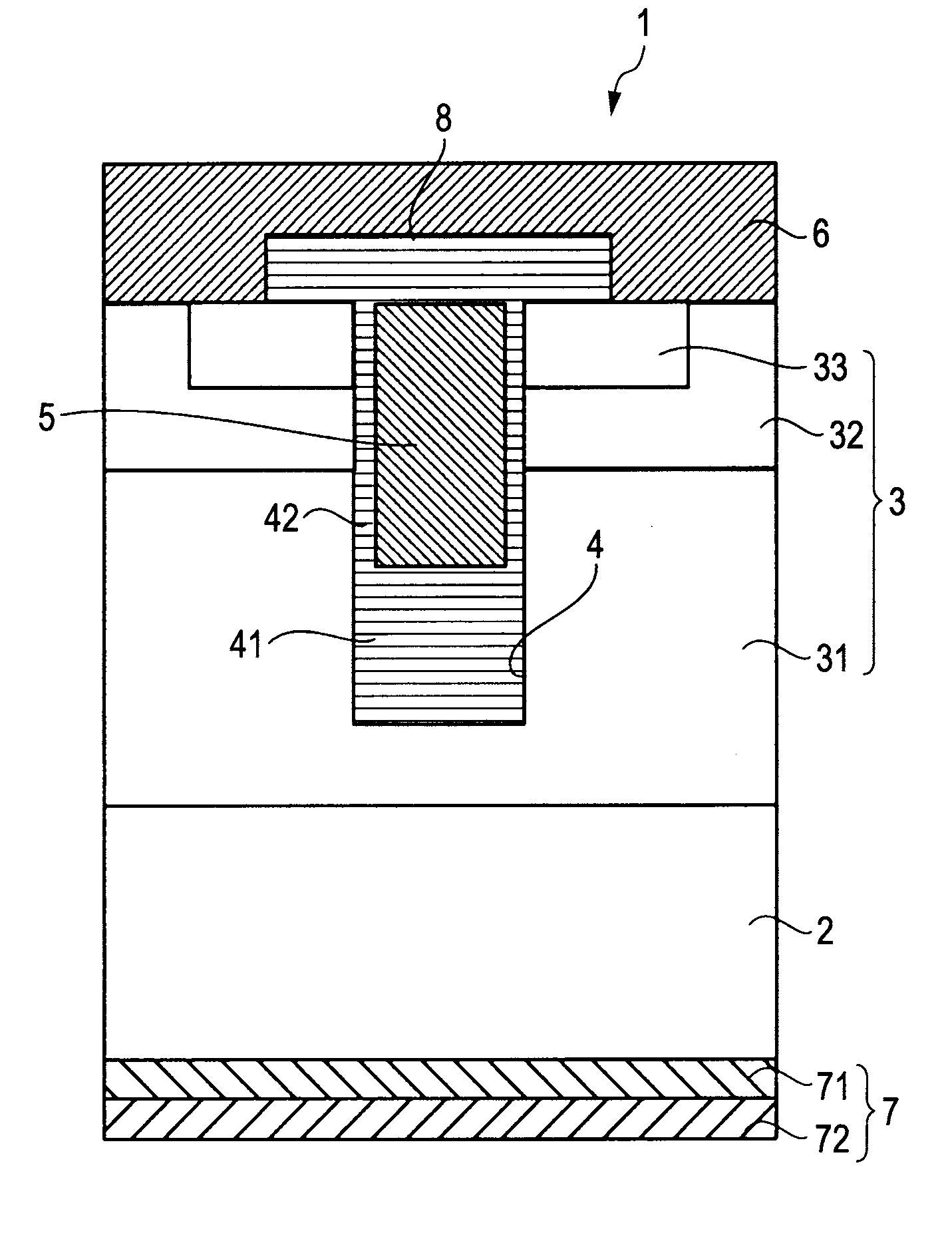
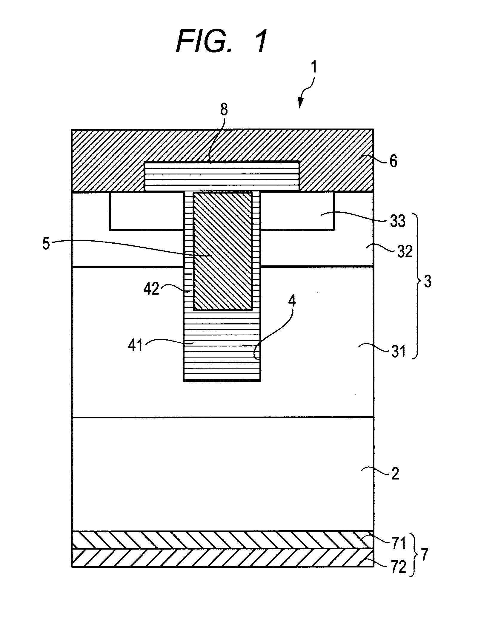
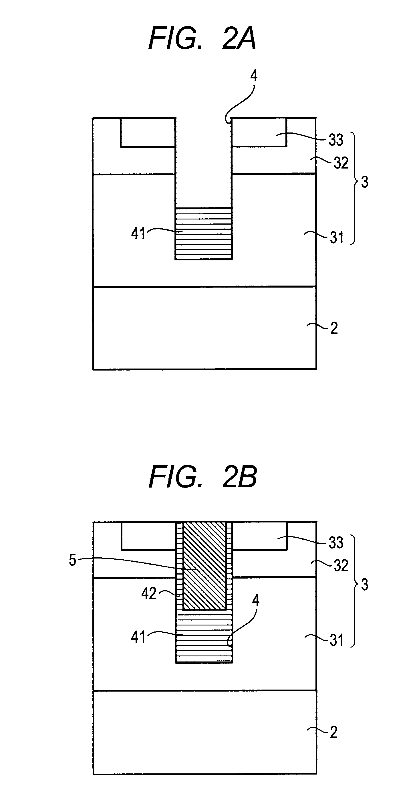
[0041]FIG. 1 shows an enlarged cross sectional view for a main portion of a semiconductor device according to Embodiment 1. The semiconductor device 1 comprises a semiconductor layer 3 in which a P− type drift region 31, an N type body region 32, a P+ type source region 33 are formed over a P type silicon substrate 2 that functions as a P type impurity diffusion layer. Further, the semiconductor device 1 comprises a trench 4, a gate electrode 5, a surface electrode 6, a back surface electrode 7, an interlayer dielectric film 8, a bottom-buried dielectric layer 41, and a gate dielectric film 42.

[0042]The P type silicon substrate 2 is a single crystal semiconductor substrate (single crystal silicon wafer) containing impurities having P conduction type (for example B (boron)). The concentration of impurities in the P type silicon substrate 2 can be set, for example, to about 1×1020 cm−3. While the resistance of the P type silicon substrate 2 is not particularly restricted, it is prefer...

embodiment 2

[0071]Then, an example of a semiconductor device different from Embodiment 1 is to be described. In the subsequent description, identical members with those of the embodiment described above and the examples of the prior art carry the same reference numerals for which the explanation is to be omitted optionally.

[0072]Embodiment 1 described above shows an example in which a metal layer having a work function of 4.5 eV or more is in contact with the P type silicon substrate. However, the present invention is applicable not being restricted only to Embodiment 1 but also applicable to a semiconductor device in which an impurity region at a higher concentration of P type impurity is formed to a P type silicon substrate or an N type silicon substrate at a lower impurity concentration by ion implantation or the like. FIG. 3B shows an energy barrier φB when an impurity region at higher concentration of P type impurity is provided to the single crystal surface of a P type silicon substrate b...

embodiment 3

[0078]FIG. 5 is an enlarged cross sectional view for a main portion of a semiconductor device 1c according to Embodiment 3. The semiconductor device 1c is an example of applying the back surface electrode 7 described above to a vertical type IGBT shown in FIG. 8. The semiconductor device 1c is an example of forming a P type emitter layer 101 that functions as a P type impurity diffusion layer to the side of the back surface of the N type base layer 102 formed of the N type silicon substrate for example by ion implantation and laser annealing and the surface is wet etched to expose the single crystal surface to which a first metal layer (for example, Ni layer) 71 having a work function of 4.5 eV or more and a second metal layer (for example, Ag layer) 72 at 120° C. or lower to form the back surface electrode 7. In a case where the impurity concentration of the entire P type emitter layer 101 cannot be increased due to the restriction of breakdown voltage, for example, a P type impuri...


PUM

PropertyMeasurementUnit
temperatureaaaaaaaaaa
work functionaaaaaaaaaa
temperatureaaaaaaaaaa

Abstract

A semiconductor device includes a vertical type semiconductor element formed by using a silicon substrate, a P type impurity diffusion layer being formed at a back surface of the silicon substrate. The surface of the P type impurity diffusion layer is wet etched to expose a single silicon crystal surface of the P type impurity diffusion layer, and a metal layer having a work function of 4.5 eV or more is disposed to the single silicon crystal surface so that an ohmic contact is made between the single silicon crystal surface of the P type impurity diffusion layer and the metal layer without making a silicon-metal alloy layer between the P type impurity diffusion layer and the metal layer.

Description

CROSS-REFERENCE TO RELATED APPLICATION[0001]The disclosure of Japanese Patent Application No. 2009-290359 filed on Dec. 22, 2009, and No. 2010-184068 filed on Aug. 19, 2010 the specification, drawings and abstract is incorporated herein by reference in its entirety.BACKGROUND[0002]1. Field of the Invention[0003]The present invention concerns a method of manufacturing a semiconductor device and the semiconductor device. More specifically, it relates to a method of manufacturing a semiconductor device for supplying a current in a vertical direction, and the semiconductor device.[0004]2. Description of Related Art[0005]Generally, in a semiconductor device controlling a large current, for example, insulated gate bipolar transistors (IGBT), metal-oxide semiconductor filed-effect transistor (MOSFET), diodes, or suchlike, an electronic circuit is formed on one surface of a silicon substrate, and a back surface electrode comprising a plurality of layers is formed at the back surface thereof...

Claims


Application Information

Patent Timeline
Patent Type & Authority Patents(United States)
IPC IPC(8): H01L21/336H01L21/46H01L21/30
CPCH01L21/0485H01L29/456H01L29/66734H01L29/7395H01L29/7397H01L29/7813H01L29/42368
Inventor YAMASAKI, JUNJI
Owner RENESAS ELECTRONICS CORP
Why Eureka
Try Eureka