Chemical amplification resist composition, and resist film, resist-coated mask blank, resist pattern forming method and photomask each using the composition

a technology of resist film and composition, which is applied in the direction of photosensitive materials, instruments, photomechanical equipment, etc., can solve the problems of resist film thinning, reducing the energy trapping ratio of resist film, and reducing the sensitivity, so as to achieve high sensitivity and high resolution. high, high resolution property

Active Publication Date: 2014-07-15
FUJIFILM CORP
View PDF16 Cites 0 Cited by
  • Summary
  • Abstract
  • Description
  • Claims
  • Application Information

AI Technical Summary

Benefits of technology

[0010]An object of the present invention is to provide a chemical amplification resist composition capable of forming a pattern satisfying high sensitivity, high resolution property (for example, high resolution, excellent pattern profile and small line edge roughness (LER)) and good dry etching resistance all at the same time, and a resist film, a resist-coated mask blank, a resist pattern forming method and a photomask each using the composition.
[0026]According to the present invention, a chemical amplification resist composition capable of forming a pattern satisfying high sensitivity, high resolution property (for example, high resolution, excellent pattern profile and small line edge roughness (LER)) and good dry etching resistance all at the same time, and a resist film, a resist-coated mask blank, a resist pattern forming method and a photomask each using the composition can be provided.

Problems solved by technology

In order to form an ultrafine pattern, thin film formation of the resist is necessary, but thinning of the resist film incurs deterioration of the dry etching resistance.
However, in this case, the electron energy trapping ratio of the resist film decreases, giving rise to reduction in the sensitivity, and the effect of scattering (back scattering) of electrons reflected on the resist substrate increases.

Method used


Image

  • Chemical amplification resist composition, and resist film, resist-coated mask blank, resist pattern forming method and photomask each using the composition
  • Chemical amplification resist composition, and resist film, resist-coated mask blank, resist pattern forming method and photomask each using the composition
  • Chemical amplification resist composition, and resist film, resist-coated mask blank, resist pattern forming method and photomask each using the composition

Examples


synthesis example 1

Synthesis of Polymer Compound (A1)

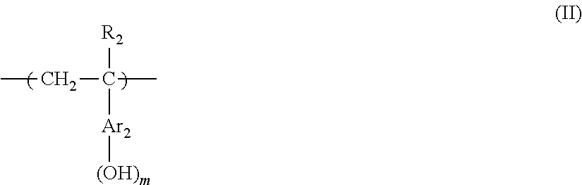
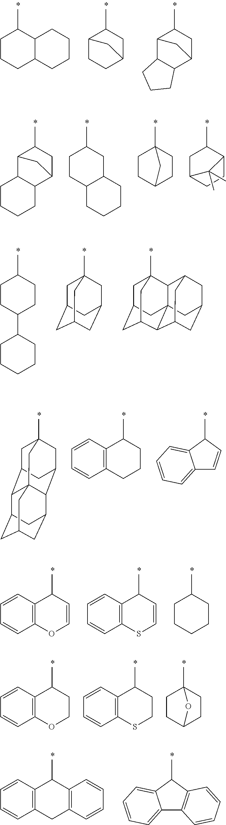
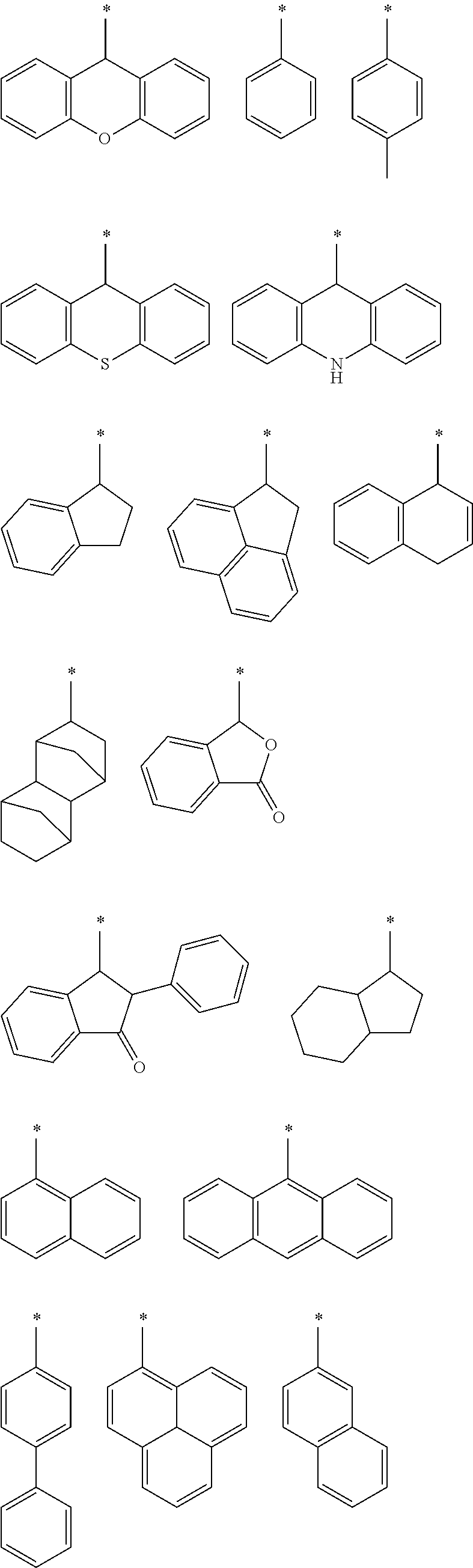
[0196]In 120 mL of tetrahydrofuran (THF), 20 g of poly(p-hydroxystyrene) (VP2500) produced by Nippon Soda Co., Ltd. was dissolved, and 4.96 g of 1-adamantanecarbonyl chloride and 3.37 g of triethylamine were added thereto. The mixture was stirred at 50° C. for 4 hours, and the reaction solution was returned to room temperature. Thereafter, 100 mL of ethyl acetate and 100 mL of distilled water were added thereto, and an aqueous 1 N HCl solution was added little by little to the reaction solution to effect neutralization while stirring the reaction solution in ice water. The reaction solution was transferred to a separating funnel, and 100 mL of ethyl acetate and 100 mL of distilled water were further added. After stirring, the aqueous layer was removed, and the organic layer was washed with 200 mL of distilled water five times. The organic layer was then concentrated and added dropwise in 2 L of hexane. After filtration, the powder was collected and ...

example 1e

(1) Preparation of Support

[0202]A Cr oxide-deposited 6-inch wafer (a wafer subjected to a treatment of forming a shielding film, which is used for normal photomask blank) was prepared.

(2) Preparation of Resist Coating Solution

[0203]

(Coating Solution Formulation of Negative Resist Composition N1)Polymer Compound (A1)0.60gPhotoacid generator (z42) (the structural formula is shown0.12gabove)Crosslinking Agent CL-1 (the structural formula is shown0.08gbelow)Crosslinking Agent CL-4 (the structural formula is shown0.04gbelow)Tetrabutylammonium hydroxide (basic compound)0.002g2-Hydroxy-3-naphthoic acid (organic carboxylic acid)0.012gSurfactant PF6320 (produced by OMNOVA)0.001gPropylene glycol monomethyl ether acetate (solvent)4.0gPropylene glycol monomethyl ether (solvent)5.0g

[0204]The solution of the formulation above was microfiltered through a membrane filter having a pore size of 0.04 μm to obtain a resist coating solution.

(3) Preparation of Resist Film

[0205]The resist coating solution...

example 2e

[Example 2E] to [Example 18E], [Comparative Example 1E] and [Comparative Example 9E]

[0216]Preparation of the resist solutions (Negative Resist Compositions N2 to N18 and Comparative Negative Resist Compositions N1 and N9), negative pattern formation and evaluations thereof were performed in the same manner as in Example 1E except that in the resist solution formulation, the components in Table 2 below were used.

[0217]

TABLE 2CrosslinkingCompositionResin / CompoundAcid GeneratorBasic CompoundAgentSolventN1Polymer compoundz42B1CL-1 / CL-4S2 / S1(A1) (0.6 g)(0.12 g)(0.002 g)(0.08 g / 0.04 g)(5.0 g / 4.0 g)N2Polymer compoundz42B1CL-1 / CL-4S1 / S3(A2) (0.6 g)(0.12 g)(0.002 g)(0.08 g / 0.04 g)(5.0 g / 4.0 g)N3Polymer compoundz42B1CL-1 / CL-4S2 / S3(A3) (0.6 g)(0.12 g)(0.002 g)(0.08 g / 0.04 g)(5.0 g / 4.0 g)N4Polymer compoundz42B1CL-1 / CL-4S2 / S7(A4) (0.6 g)(0.12 g)(0.002 g)(0.08 g / 0.04 g)(5.0 g / 4.0 g)N5Polymer compoundz42B1CL-1 / CL-4S2 / S1(A5) (0.6 g)(0.12 g)(0.002 g)(0.08 g / 0.04 g)(5.0 g / 4.0 g)N6Polymer compoundz67B...


PUM

PropertyMeasurementUnit
mol%aaaaaaaaaa
polydispersityaaaaaaaaaa
thicknessaaaaaaaaaa

Abstract

A chemical amplification resist composition contains: (A) a polymer compound having a phenolic hydroxyl group and a group formed by substituting a substituent for a hydrogen atom of a hydroxyl group in a phenolic hydroxyl group and satisfying the following (a) to (c) at the same time: (a) the polydispersity is 1.2 or less, (b) the weight average molecular weight is from 2,000 to 6,500, and (c) the glass transition temperature (Tg) is 140° C. or more.

Description

BACKGROUND OF THE INVENTION[0001]1. Field of the Invention[0002]The present invention relates to a chemical amplification resist composition suitably usable in the ultramicrolithography process such as production of VLSI or high-capacity microchip as well as in other photofabrication processes and capable of forming a highly defined pattern by using an electron beam or an extreme-ultraviolet ray, and a pattern forming method using the composition. More specifically, the present invention relates to a chemical amplification resist composition for use particularly in the process using a substrate having a specific underlying film, and a resist film, a resist-coated mask blank, a resist pattern forming method and a photomask each using the composition.[0003]2. Description of the Related Art[0004]In the microfabrication using a resist composition, with an increase in the integration degree of an integrated circuit, formation of an ultrafine pattern is required. To meet this requirement,...

Claims


Application Information

Patent Timeline
Patent Type & Authority Patents(United States)
IPC IPC(8): G03F7/038G03F1/00G03F7/20G03F7/30
CPCC08F12/24C08F12/18C08F12/20C08F12/30C08F212/14C08F212/32C09D125/18G03F1/56G03F1/76G03F7/0382C08F212/24C08F212/22G03F1/00G03F7/004G03F7/0045G03F7/11G03F7/20G03F7/202G03F7/26G03F1/50
Inventor TSUCHIMURA, TOMOTAKAYATSUO, TADATERU
Owner FUJIFILM CORP
Why Eureka
Try Eureka