Devices and systems for power conversion circuits

a power conversion circuit and power conversion circuit technology, applied in the direction of electronic switching, pulse technique, basic electric elements, etc., can solve the problems of shortening the potential capabilities of individual gan transistors, shortening the overall performance of hybrid cascode arrangements using existing driver circuits, and unwanted switching, so as to reduce series inductance and resistance, effective thermal management

Active Publication Date: 2015-08-11
GAN SYST
View PDF5 Cites 9 Cited by
  • Summary
  • Abstract
  • Description
  • Claims
  • Application Information

AI Technical Summary

Benefits of technology

[0030]The respective arrangements of front-side / on-chip contacts areas of the CMOS die and the GaN die are matched (i.e. mirror image) to provide for direct interconnection of respective contact areas by conductive interconnects when the two die are stacked in a flip-chip configuration. Advantageously, each respective pair of contact areas of the CMOS die and GaN die is interconnected by a conductive interconnect comprising a low inductance, low resistance interconnect material, e.g. micro-connects comprising metal posts, such as copper. This arrangement for assembly and co-packaging enables a compact and low inductance, low capacitance connection between the CMOS die carrying the CMOS driver circuit and integrated driver MOSFET and the GaN.
[0036]As described in detail in the above referenced U.S. provisional application No. 61 / 740,825, an integrated CMOS driver circuit provides for more complex control and monitoring of the power transistor. The driver circuit is configured to reduced noise and reduces unwanted voltage transients, using latch and clamp control circuitry based on monitoring Vcc conditions. It provides for power-up and power-down conditioning for safer operation Isolation is preferably provided by an isolation transformer coupling, and an integrated power source is also desirably, eliminating the need for separate isolation and a separate power source.
[0039]Thus, arrangements are disclosed for co-packaging and interconnection of a hybrid cascode arrangement of a normally-on HV GaN FET and a normally-off driver MOSFET that reduces series inductance and resistance, and provides effective thermal management.
[0040]Thus, devices and systems are provided comprising a cascode arrangement of a GaN power transistor and a driver MOSFET integrated with a CMOS driver circuit. Advantageously, embodiments of the system mitigate or circumvent one or more limitations of known devices and systems.

Problems solved by technology

However, issues caused by transient voltages and heat dissipation can detract from performance and these issues also create challenges for the design of the driver circuit.
The overall performance of hybrid cascode arrangements using existing driver circuits falls short of the potential capabilities of an individual GaN transistor.
Any significant series inductance at the MOSFET source or at the common node will provide unwanted L di / dt transients which can be as large as the threshold voltage of the devices, thus causing unwanted switching.
Additionally, series resistance in the source connection results in debiasing which produces an apparent increase in the on-resistance.
Wire bonding is expensive, area consuming, and cumbersome.
Additionally, the wire bonded interconnects represent significant inductance that contributes to high frequency switching transients and unnecessary power loss, particularly for switching speeds in the order of 100V / ns.
This arrangement then presents problems for thermal management.
Thus, conventional cascode arrangements of a GaN power transistor and a discrete driver MOSFET require complex and costly driver circuitry to manage issues with transient voltages and packaging with significant thermal dissipation capability to maintain acceptable operating temperatures.

Method used


Image

  • Devices and systems for power conversion circuits
  • Devices and systems for power conversion circuits
  • Devices and systems for power conversion circuits

Examples


first embodiment

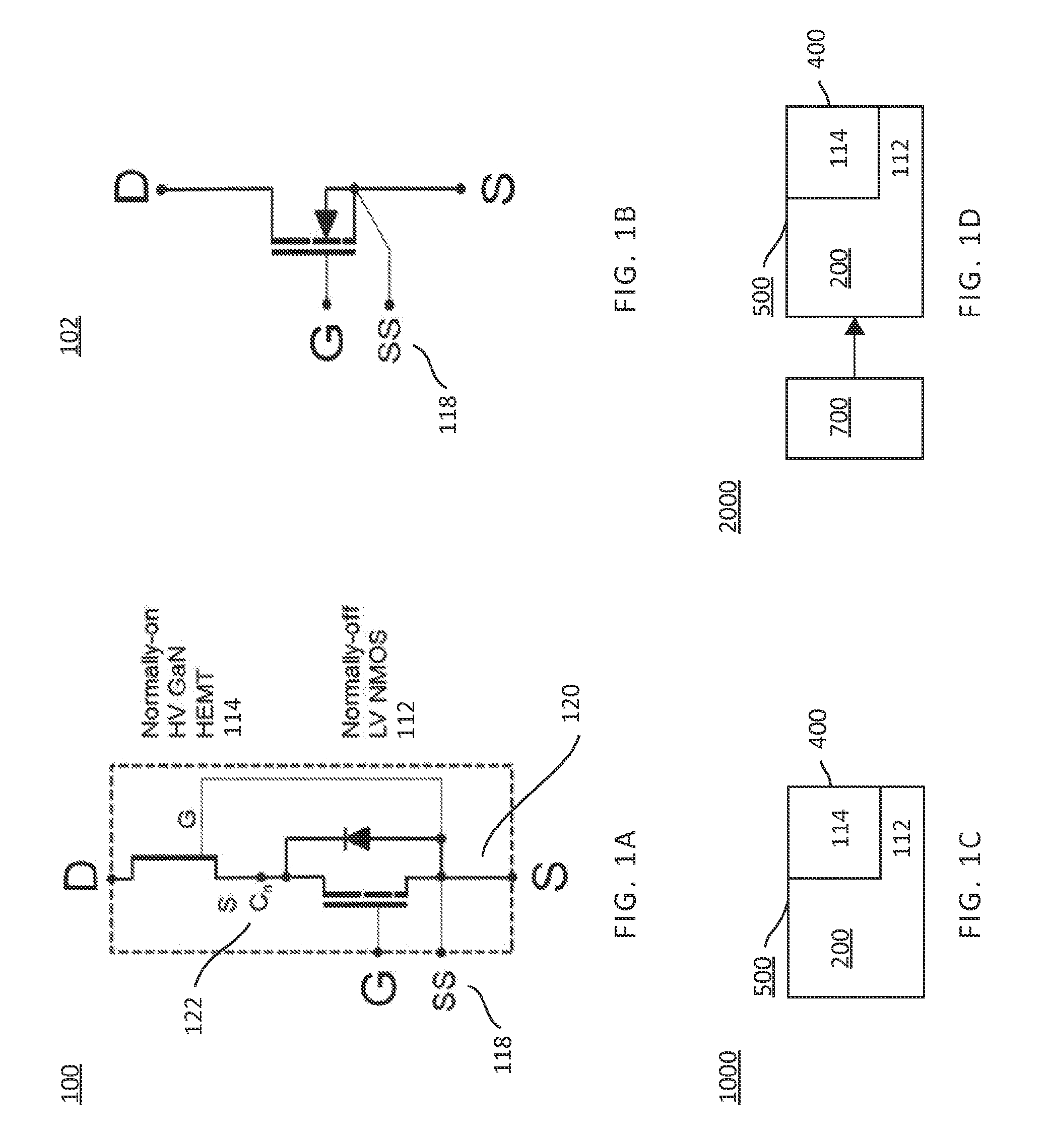
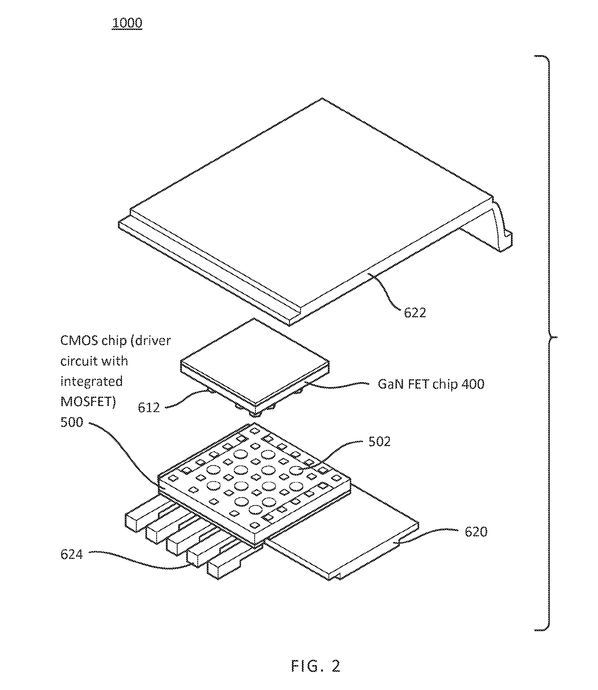
[0059]FIG. 1C shows a simplified block diagram of a system 1000 according to the present invention comprising a cascode arrangement of a normally-on (depletion mode) HV GaN power transistor 114 and a normally-off LV MOSFET driver 112 transistor, comprising an assembly of a first die (GaN die) 400, comprising the GaN power transistor 114 and a second die (CMOS driver die) 500, comprising a CMOS driver circuit 200 with an integrated driver MOSFET 112.

[0060]FIG. 1D shows a simplified block diagram of a system according to a second embodiment comprising a cascode arrangement of a normally-on (depletion mode) HV GaN power transistor and a normally-off LV MOSFET driver transistor, comprising an assembly of a first die comprising the GaN power transistor (GaN die); a second die (CMOS driver die) comprising a CMOS driver circuit with an integrated driver MOSFET; and a third die comprising an interface circuit for pre-isolation conditioning and isolation. FIG. 2 shows an exploded view of ele...

second embodiment

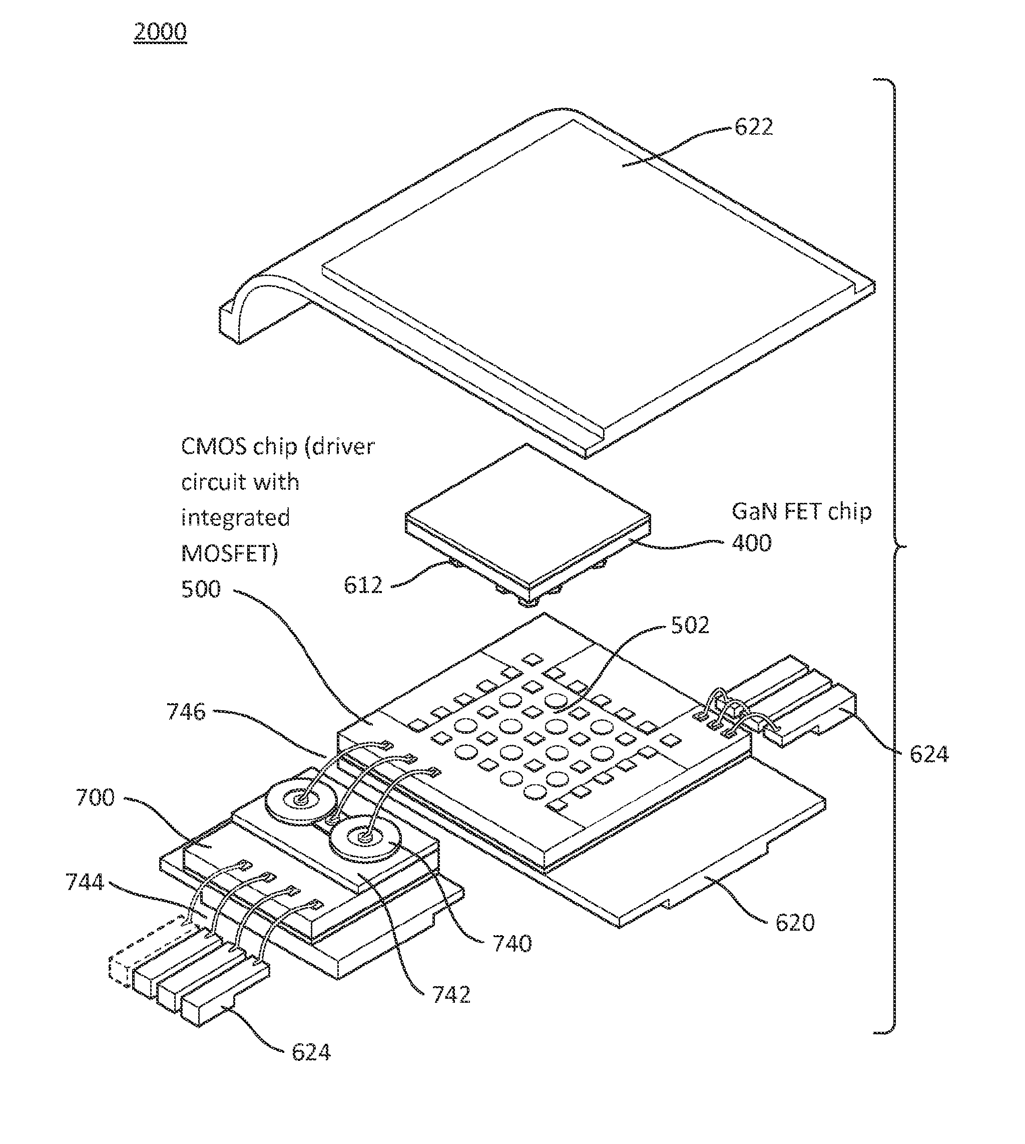
[0085]An exploded view of elements of a system 2000 according to the invention is shown in FIG. 7.

[0086]The system 2000 is similar to the system 1000 shown in FIG. 2, and similarly provides for direct interconnection of the GaN FET die 400 and the CMOS driver die 500, comprising an integrated driver MOSFET. Additionally, it comprises another die, comprising an interface circuit 700, coupled to the inputs of the CMOS driver die 500. Details of the design and operation of interface circuit 700 are also described in detail in the above referenced related copending US provisional patent application. The interface circuit 700 provides pre-isolation conditioning and isolation within the same package. The interface circuit 700 is fabricated as a CMOS integrated circuit comprising a pulse generator and an isolation transformer coupling, for coupling differential input control signals to the CMOS driver chip. The interface circuit may for example comprise a substrate based transformer with a...


PUM

PropertyMeasurementUnit
breakdown voltageaaaaaaaaaa
current switching capabilityaaaaaaaaaa
threshold voltageaaaaaaaaaa

Abstract

Devices and systems comprising driver circuits are disclosed for MOSFET driven, normally-on gallium nitride (GaN) power transistors. Preferably, a low power, high speed CMOS driver circuit with an integrated low voltage, lateral MOSFET driver is series coupled, in a hybrid cascode arrangement to a high voltage GaN HEMT, for improved control of noise and voltage transients. Co-packaging of a GaN transistor die and a CMOS driver die using island topology contacts, through substrate vias, and a flip-chip, stacked configuration provides interconnections with low inductance and resistance, and provides effective thermal management. Co-packaging of a CMOS input interface circuit with the CMOS driver and GaN transistor allows for a compact, integrated CMOS driver with enhanced functionality including shut-down and start-up conditioning for safer operation, particularly for high voltage and high current switching. Preferred embodiments also provide isolated, self-powered, high speed driver devices, with reduced input losses.

Description

CROSS-REFERENCE TO RELATED APPLICATION(S)[0001]This application claims priority from U.S. provisional patent application No. 61 / 740,821, filed 21 Dec. 2012, entitled “Devices and Systems for Power Conversion Circuits” and from U.S. Provisional patent application No. 61 / 740,825, filed 21 Dec. 2012, entitled “Devices and Systems comprising Drivers for Power Conversion Circuits”, filed 21 Dec. 2012; both applications are incorporated herein by reference in their entirety.TECHNICAL FIELD[0002]This invention relates to devices and systems for electronic power conversion circuits, and more particularly relates to devices and systems comprising driver circuits for high frequency, switched mode, power conversion circuits, using high performance power transistors, such as, gallium nitride high electron mobility transistors (GaN HEMTs).BACKGROUND ART[0003]Semiconductor devices based on gallium nitride (GaN) technology offer significant advantages over silicon technology for power electronic s...

Claims


Application Information

Patent Timeline
Patent Type & Authority Patents(United States)
IPC IPC(8): H01L25/18H01L23/495H01F19/08H01L23/00H01L23/64
CPCH01L25/18H01L23/49562H01L24/06H01L23/49524H01L23/49575H01L2224/16145H01L2924/30107H01L2924/00H01L2924/1306H01F19/08H01L23/645H01L24/05H01L24/13H01L24/16H01L24/32H01L24/48H01L24/49H01L2224/0401H01L2224/04042H01L2224/05554H01L2224/05555H01L2224/0557H01L2224/06051H01L2224/06131H01L2224/06181H01L2224/13147H01L2224/32245H01L2224/48137H01L2224/48195H01L2224/48247H01L2224/49175H01L2224/73253H01L2224/73265H01L2924/10253H01L2924/10272H01L2924/1033H01L2924/13064H01L2924/13091H01L2924/19104H01L2924/00012H01L23/49548H01L2924/15747H01L2924/1305H01L2924/12035H01L2924/1204H01L24/73H01L2924/181H01L2224/49107H01L2924/00014H01L2224/40245H03K17/687H01L2224/73221H01L2224/0603H01L2224/45099H01L2224/45015H01L2924/207
Inventor ROBERTS, JOHNKLOWAK, GREG
Owner GAN SYST
Why Eureka
Try Eureka