Chemical passivation method for measuring minority carrier lifetime of crystalline silicon

A chemical passivation, minority carrier lifetime technology, used in semiconductor/solid-state device testing/measurement, single semiconductor device testing, semiconductor/solid-state device manufacturing, etc. and other problems, to achieve the effect of low cost, reduction of high temperature diffusion process, and simple post-processing process

Inactive Publication Date: 2009-11-18
BAODING GUANGWEI GREEN ENERGY TECH CO LTD
View PDF2 Cites 2 Cited by
  • Summary
  • Abstract
  • Description
  • Claims
  • Application Information

AI Technical Summary

Problems solved by technology

[0010] The purpose of the present invention is to overcome the following shortcomings in the prior art: complex chemical cleaning process in the early stage, high-temperature oxidation process and plasma deposition film process of high energy consumption and likely to reduce the bulk performance of crystalline silicon, and other chemical passivation processes. In order to avoid the operational complexity of the crystalline silicon method and the pollution caused by the test crystalline silicon, a method for chemical passivation of the crystalline silicon is provided.

Method used


Image

  • Chemical passivation method for measuring minority carrier lifetime of crystalline silicon
  • Chemical passivation method for measuring minority carrier lifetime of crystalline silicon
  • Chemical passivation method for measuring minority carrier lifetime of crystalline silicon

Examples


Embodiment 1

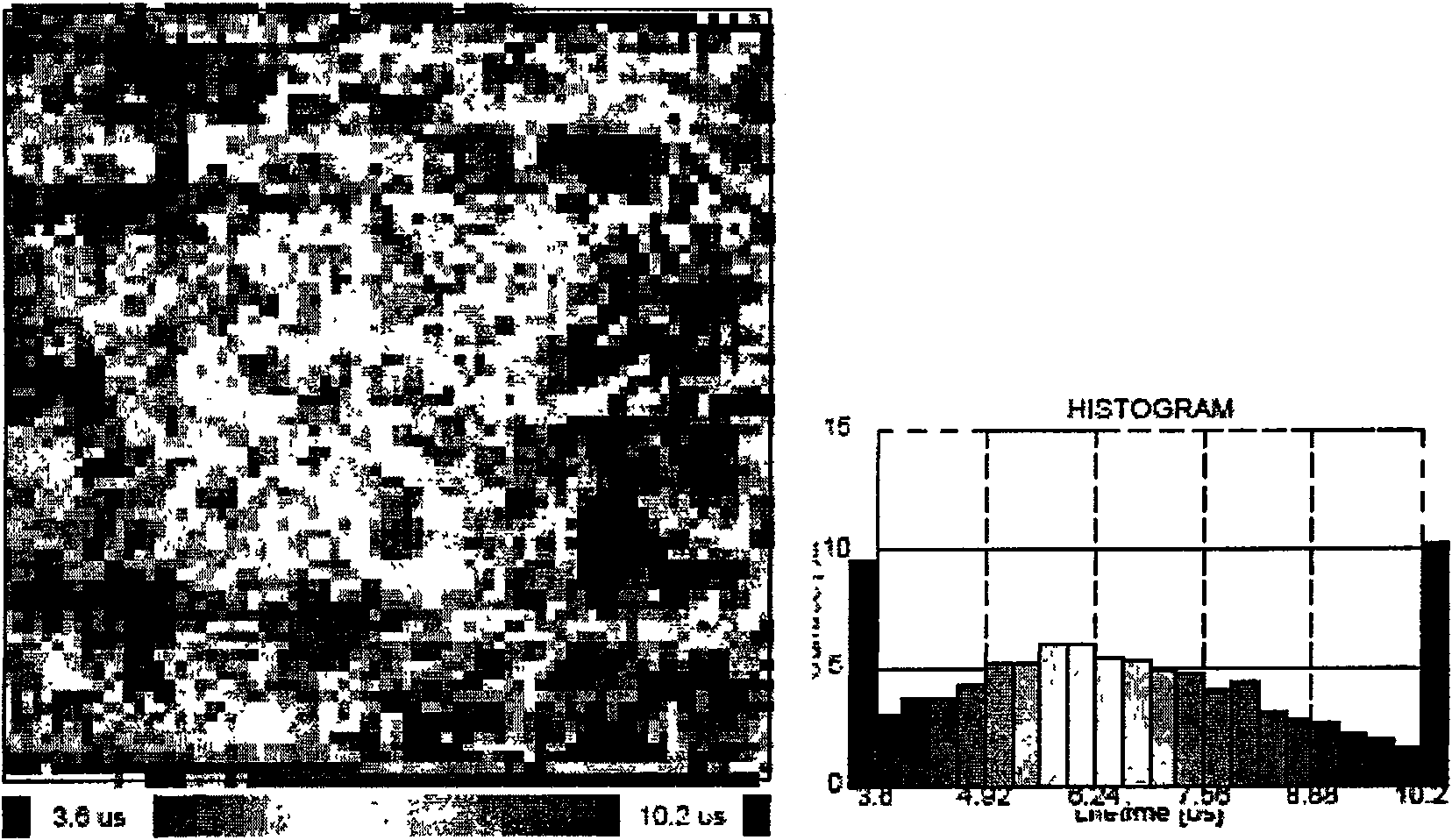
[0035] Take a P-type Czochralski monocrystalline silicon wafer imported from Korea, with a resistivity of 15 ohm cm, a thickness of 700 microns, and double-sided polishing. Two slices A and B were cut on the same silicon wafer. Since the two slices A and B are polished slices, there is no damage removal process. Carry out direct measurement respectively to A, B two respectively: the hydrogen fluoride passivation measurement of the present invention, and the iodine passivation test in United States Patent, patent number5580828.

[0036] Direct chip test: Two chips are placed directly on the sample stage of the microwave photoconductive attenuation quantum lifetime tester without any treatment, and then the minority carrier lifetime is tested to obtain the plane distribution of the minority carrier lifetime, and finally the average value of the crystalline silicon is obtained. Minor life expectancy.

[0037] High-concentration HF passivation among the present invention: 1) the ...

Embodiment 2

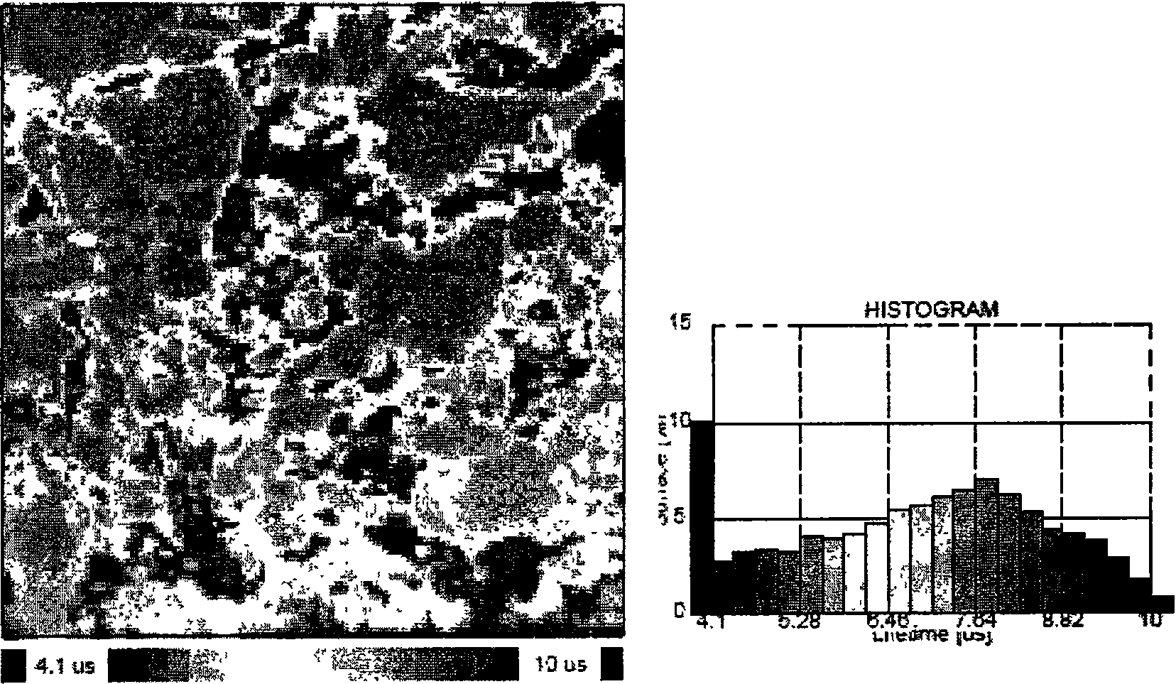
[0042] For P-type (100), cast polysilicon wafers with a resistivity of 1Ωcm and a thickness of 220 μm, phosphorus diffusion passivation is compared with the passivation method of the present invention. Firstly, the polysilicon wafer is pre-treated to remove damage: use hydrogen fluoride (HF) (39%): HNO 3 (75%):CH 3 A mixed solution of COOH (99%)=1:3:3 (volume ratio) was used to remove the damaged layer on two polysilicon wafers cut from the same cast polysilicon wafer at room temperature, and the etching time of the solution was 20 minutes. Then the two pieces were subjected to diffusion passivation and hydrogen fluoride (HF) solution passivation test in the present invention respectively.

[0043] One of the polycrystalline silicon wafers after the damage is removed is subjected to a passivation test according to the passivation method in the present invention: 1) the rinsed wafer is rinsed for 30s in a 20% concentration of diluted hydrogen fluoride (HF) solution; 2) the cry...

Embodiment 3

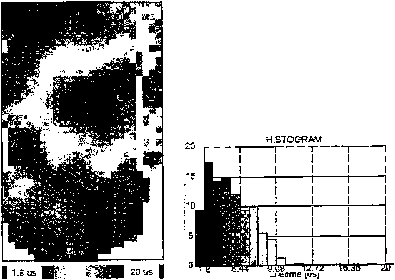
[0046] Utilize the passivation method of the present invention and United States Patent, the 1% iodine solution in patent number 5580828 carries out the test and comparison of the minority carrier life of the monocrystalline silicon wafer used in industrialized solar cell production respectively, P type (100) single crystal Silicon, resistivity 1Ωcm, thickness 220μm. This kind of sheet also has a 10-20 μm thick damaged layer on the surface, so pretreatment to remove the damaged layer is also required. The monocrystalline silicon wafer is put into the damage-removing and texturing equipment in the industrial production line, and the damage-removing and texturing are performed according to the conventional production process, and the textured wafer is taken out. Then according to the present invention and United States Patent respectively, 1% iodine solution (1g iodine is put in the dehydrated alcohol of 100ml) passivation in the patent number 5580828, the crystalline silicon ch...


PUM


Abstract

The invention discloses a chemical passivation method for measuring the service life of a minority carrier of crystalline silicon, wherein, a silicon chip after finishing damage-layer removing process is washed by a high-concentration hydrogen fluoride solution of 39 percent or 49 percent concentration diluted by de-ionized water in a normal temperature to remove the natural oxide on the surface of the silicon chip; then the silicon chip is put in a transparent, hydrogen fluoride (HF) resistant plastic bag free of electrical signal interference, and drops of hydrogen fluoride (HF) solution of 39 percent concentration are dropped on the front and the rear surfaces of the crystalline silicon, and then the hydrogen fluoride solution on the silicon chip is needed to be flatted outside the plastic bag to make the thickness of the hydrogen fluoride solution less than 1mm; finally the air bubbles rudimental on the silicon chip are removed. After sealed by a plastic sealing machine, the plastic bag is put on a sample table of a measuring device for measuring. The invention can achieve the even passivation effect of the surface of the silicon chip, and reduces the composition speed of the surface under 100cm / s, and the invention is of low cost, easy operation, time-saving measurement, and is particularly suitable for measuring and analyzing raw silicon chip materials in solar battery production and research department.

Description

technical field [0001] The invention relates to a method for passivating the surface of crystalline silicon with a chemical solution for testing the minority carrier lifetime of crystalline silicon. Background technique [0002] Minority carrier lifetime (referred to as bulk minority carrier lifetime) is an important parameter of semiconductor crystalline silicon materials, which has an important impact on the performance of semiconductor devices and the photoelectric conversion efficiency of crystalline silicon solar cells. In solar cells, the lifetime value determines the stable number of electrons and holes when carriers are continuously generated. These numbers determine the voltage generated by the device and therefore require that the minority carrier lifetime of the crystalline silicon body of the silicon material used should be as high as possible. It is precisely because the bulk minority carrier lifetime of the crystalline silicon used is directly related to the e...

Claims


Application Information

Patent Timeline
Patent Type & Authority Patents(China)
IPC IPC(8): H01L21/314H01L21/306H01L21/66G01R31/26
Inventor 周春兰王文静唐煜李海玲
Owner BAODING GUANGWEI GREEN ENERGY TECH CO LTD
Why Eureka
Try Eureka