Controllable asymmetric doping potential barrier nano silicon based luminous device and method for producing the same

A light-emitting device, nano-silicon technology, applied in semiconductor devices, electrical components, circuits, etc., can solve problems such as carrier injection imbalance

Inactive Publication Date: 2008-09-24
NANJING UNIV
View PDF0 Cites 14 Cited by
  • Summary
  • Abstract
  • Description
  • Claims
  • Application Information

AI Technical Summary

Problems solved by technology

The above methods all improve the injection efficiency of carriers from the electrode to the light-emitting active layer, but, as far as the applicant knows, there is no effective solution to the current-carrying problem caused by the difference in the energy band shift of the conduction band and the valence band. Method for sub-injecting unbalanced problems

Method used


Image

  • Controllable asymmetric doping potential barrier nano silicon based luminous device and method for producing the same
  • Controllable asymmetric doping potential barrier nano silicon based luminous device and method for producing the same
  • Controllable asymmetric doping potential barrier nano silicon based luminous device and method for producing the same

Examples


Embodiment 1

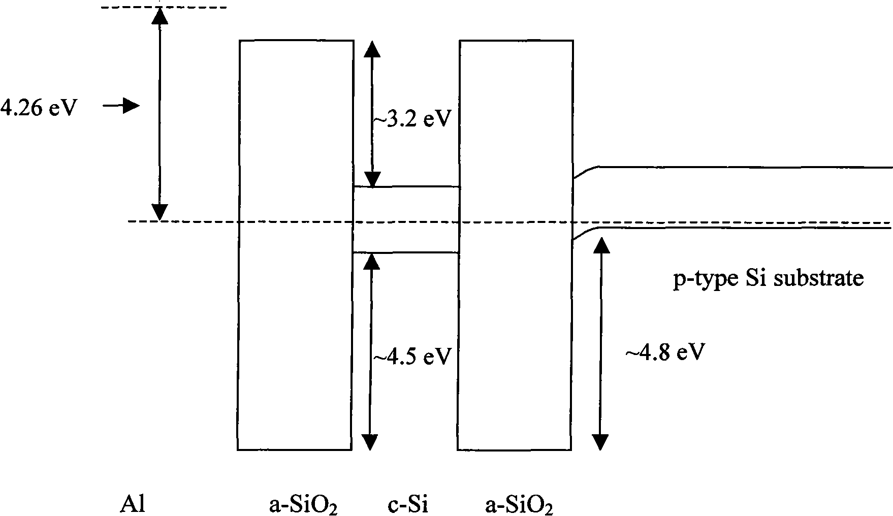
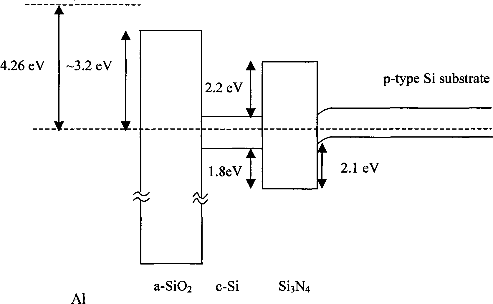
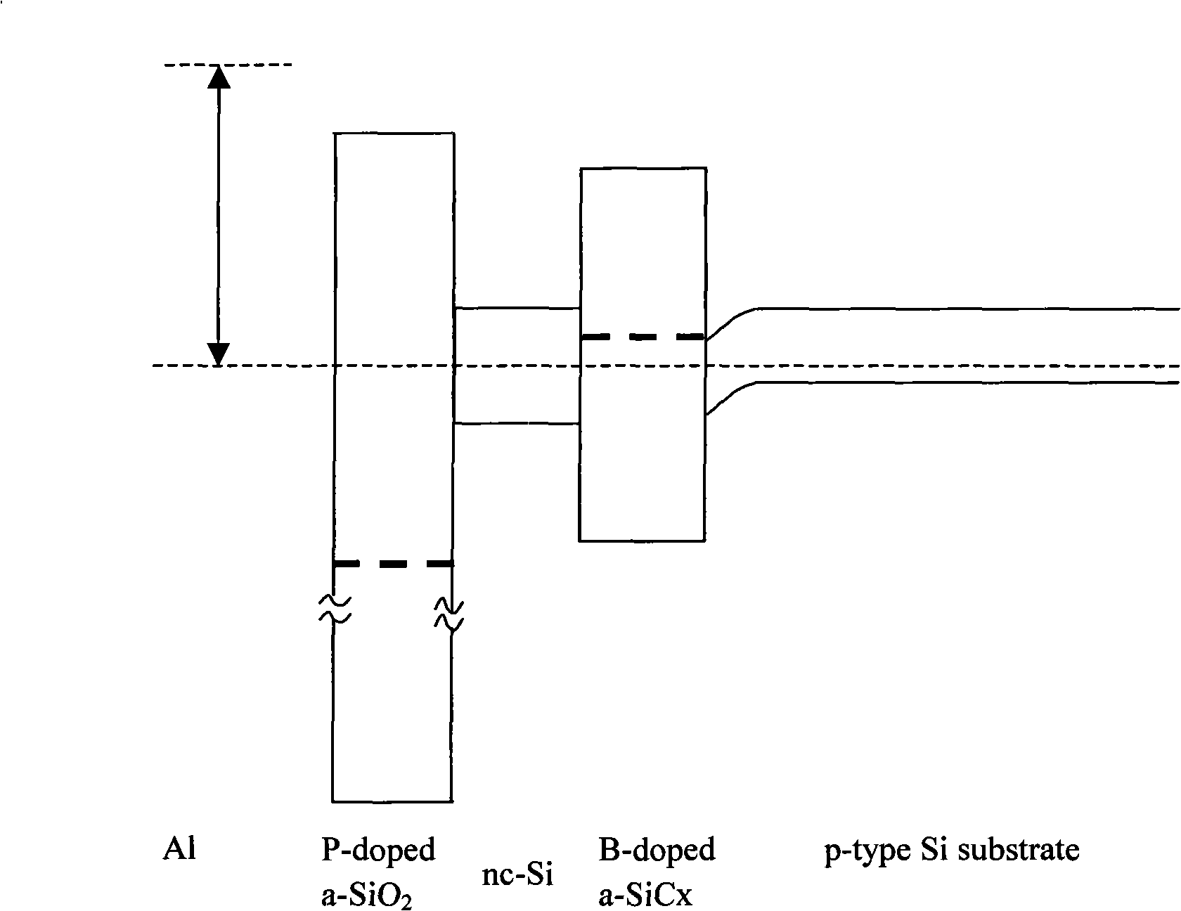
[0053] The controllable asymmetric doped barrier nano-silicon light-emitting device in this embodiment uses Al / P-doped a-SiO 2 / nc-Si / B-doped a-SiCx / p-type Si device structure, the preparation process is as follows:

[0054] The first step is to prepare a multi-layer film with a quantum well structure by using plasma-enhanced chemical vapor deposition (PECVD) technology

[0055] 1-1. Preparation of boron-doped hydrogenated amorphous silicon carbide (B-doped a-SiCx:H) film as a barrier layer: using a flat capacitive RF plasma-enhanced chemical vapor deposition (PECVD) system, the substrate is placed in the reaction On the metal anode plate grounded in the chamber, silane (SiH 4 ), methane (CH 4 ) and borane (B 2 h 6 ) (borane diluted with hydrogen, with a concentration of 1%) as a reactive gas source, to deposit a boron-doped a-SiCx:H film with a thickness of no more than 10 nm (for example, 0.2-10 nm). During deposition, the gas flow ratio is preferably SiH 4 :CH 4 :B ...

Embodiment 2

[0069] The controllable asymmetric doped barrier nano-silicon-based light-emitting device and its preparation method in this embodiment use ITO (indium tin oxide) / B-doped a-SiCx / nc-Si / P-dopeda-SiO 2 / n-type Si device structure, the implementation process is as follows:

[0070] The first step, using plasma enhanced chemical vapor deposition (PECVD) technology to prepare multilayer films with quantum well structure

[0071] 1-1. Preparation of phosphorous hydrogenated amorphous silicon (P-doped a-Si:H) thin film: using a flat capacitive radio frequency plasma enhanced chemical vapor deposition (PECVD) system, the n-type substrate is placed in a grounded reaction chamber On the metal anode plate, silane (SiH 4 ) and phosphine (PH 3 ) (phosphine diluted with hydrogen, the concentration is 1%) as a reaction gas source, continue to deposit a 0.1-5nm thick phosphorus-doped hydrogenated amorphous silicon film on the hydrogenated amorphous silicon (a-Si:H) film . During deposition...


PUM

PropertyMeasurementUnit
thicknessaaaaaaaaaa
thicknessaaaaaaaaaa
thicknessaaaaaaaaaa

Abstract

The invention relates to an nc-Si based luminescent device based on a controllable asymmetric quantum well structure doping with voltage barrier and a preparation method thereof, which belongs to the technical field of nano-electronics and nano-photoelectronic device material. The luminescent device is deposited with an amorphous carborundum thin film doping with boron as a cavity barrier layer on a semiconductor substrate; the cavity barrier layer is deposited with an nc-Si film which is generated by the anneal of an amorphous silicon film and is used as a luminescent active layer; the luminescent active layer is deposited with an amorphous silicon dioxide thin film doping with phosphor which is used as an electronic barrier layer; the electronic barrier layer is deposited with a conductive film which is left with an optical window and used as the cathode of the luminescent device, while the back side of the semiconductor substrate is deposited with a conductive film which is used as the anode of the luminescent device. The technical process of the invention relates to that a multi-layer film with the quantum well structure is prepared; then annealing and crystallization are processed and the electrodes of the device are prepared. The luminescent device has the advantages of high efficient and balanced current carrier injection structure and the Si / SiO2 luminescent system, which provides the possibility of the realization of a high efficient Si-based luminescent device.

Description

technical field [0001] The invention relates to a silicon-based light-emitting device, especially a nano-silicon-based light-emitting device based on a controllable asymmetric doping barrier quantum well structure, and also relates to a preparation method thereof, belonging to the technical field of nano-electronics and nano-optoelectronic device materials . Background technique [0002] Silicon-based microelectronics technology has become the basis of modern electronic technology, created today's rapidly developing information age, and caused great changes in social life. However, with the continuous improvement of the integration of microelectronic devices, the existing devices will reach their physical limits and face many new challenges such as physical mechanisms, time delays, and processes. In the above background, people's attention has turned from electrons to photons, trying to use photons as information carriers. However, in the field of optoelectronic integratio...

Claims


Application Information

Patent Timeline
Patent Type & Authority Applications(China)
IPC IPC(8): H01L33/00
Inventor 韦德远徐骏王涛陈德媛韩培高孙红程刘宇陈谷然陈坤基马忠元李伟徐岭
Owner NANJING UNIV
Why Eureka
Try Eureka