Method for growing p-type AlGaN

A p-type, growth temperature technology, applied in the direction of sustainable manufacturing/processing, final product manufacturing, coating, etc., can solve the problems of difficult to obtain electrical conductivity, increase of dislocation density, high activation energy of Mg, and achieve improved surface morphology Appearance, increased luminous intensity, and reduced sheet resistance

Inactive Publication Date: 2010-06-09
PEKING UNIV
View PDF0 Cites 10 Cited by
  • Summary
  • Abstract
  • Description
  • Claims
  • Application Information

AI Technical Summary

Problems solved by technology

However, since the band gap of AlGaN widens with the increase of Al composition, the activation energy of Mg in p-AlGaN is high, and it is difficult to obtain p-type
Moreover, with the increase of the Al composition, the dislocation density of the AlGaN material itself increases, and the high-density point defects and line defects form a p-type compensation center, which further prevents the improvement of its electrical conductivity.

Method used


Image

  • Method for growing p-type AlGaN
  • Method for growing p-type AlGaN
  • Method for growing p-type AlGaN

Examples


Embodiment 1

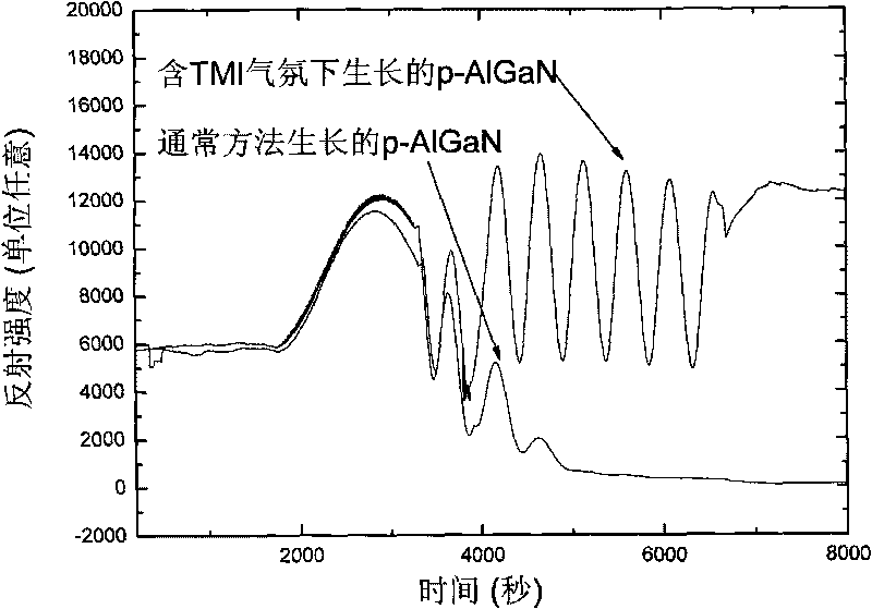
[0021] Such as figure 1 The preparation steps of the p-AlGaN sample shown are as follows:

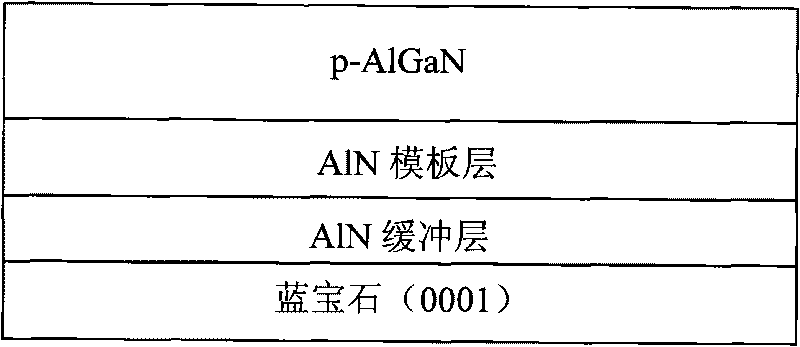
[0022] 1) The temperature of the reaction chamber is raised to 1060°C, and the sapphire (0001) substrate is baked in a hydrogen atmosphere for 15 minutes;

[0023] 2) Raise the temperature of the reaction chamber to 1200°C, and directly grow a 320nm AlN thin film on the sapphire substrate as a template layer at a growth rate of 1.4 μm per hour. The growth conditions are: pressure 50torr, V / III 400;

[0024] 3) keep the growth temperature constant, on the basis of step 2), set the flow rate of TMI to be 200 sccm, Cp 2 The flow rate of Mg is 400sccm, using TMA, TMG, TMI, Cp 2 Mg and NH 3 At the same time, the method of entering the reaction chamber grows a p-AlGaN film with a thickness of 1 μm at a growth rate of 1 μm per hour, where the Al composition is set to 0.45, and the growth conditions are: pressure 75torr, V / III is 2000.

[0025] Compared with the p-AlGaN sample grown by the ...

Embodiment 2

[0027] Such as image 3 The preparation steps of the p-AlGaN sample with the structure shown are as follows:

[0028] 1) The temperature of the reaction chamber is raised to 1060°C, and the sapphire (0001) substrate is baked in a hydrogen atmosphere for 15 minutes;

[0029] 2) Raise the temperature of the reaction chamber to 1200°C, and grow a 100-cycle AlN buffer layer on the sapphire substrate at a growth rate of 200nm per hour by pulsed atomic layer epitaxy, with a thickness of 100nm. The growth conditions are: pressure 150torr, V / III is 600, 5s TMA / 3s Hydrogen / 5s NH per cycle 3 / 3s hydrogen;

[0030] 3) Keep the temperature constant, grow a 320nm thick AlN film on the buffer layer as a template layer at a growth rate of 1.4 μm per hour, and the growth conditions are: pressure 50torr, V / III is 400;

[0031] 4) keep the growth temperature constant, on the basis of step 3), set the flow rate of TMI to be 120 sccm, Cp 2 The flow rate of Mg is 400sccm, using TMA, TMG, TMI,...

Embodiment 3

[0034] Such as Figure 5 The LED device with the structure shown, its preparation steps are as follows:

[0035] 1) The temperature of the reaction chamber is raised to 1060°C, and the sapphire substrate is heated and baked under a hydrogen atmosphere for 15 minutes;

[0036] 2) Raise the temperature to 1200°C, grow a 320nm thick AlN template layer, growth conditions: pressure 150torr, V / III is 600;

[0037] 3) Keeping the temperature constant, grow a 1 μm thick n-type AlGaN layer as a contact layer on the basis of step 2), wherein the Al component is 0.6, and the growth conditions are: pressure 75 torr, V / III is 1500, silane flow rate is 1 sccm;

[0038] 4) keep the temperature constant, and grow 3 cycles of Al on the basis of step 3)0.4 Ga 0.6 N / Al 0.25 Ga 0.75 N quantum well, the growth conditions are: pressure 75torr, V / III is 2000;

[0039] 5) Keeping the temperature constant, on the basis of step 4), a p-AlGaN electron barrier layer with a thickness of 10 nm is gro...


PUM

PropertyMeasurementUnit
thicknessaaaaaaaaaa
thicknessaaaaaaaaaa

Abstract

The invention discloses a method for growing p-type AlGaN. The method comprises the following steps: introducing trimethylindium serving as an activating agent while growing a p-type AlGaN layer by a metal organic chemical vapor deposition method, generally adopting high-purity hydrogen gas as carrier gas, trimethylgallium, trimethyl aluminium and ammonia gas as a Ga source, an Al source and an N source respectively and magnesium as a p-type doping agent, introducing the trimethylindium and other raw materials into a reaction chamber for epitaxially growing p-AlGaN, and generally controlling the flow rate of the trimethylindium to between 20 and 300 sccm. The method is simple and feasible, has obvious effect, can improve the surface appearance of the p-AlGaN, and reduces square resistance of the p-AlGaN; moreover, when applied to the preparation of a device, the method can effectively reduce the series resistance and cut-in voltage of the device, enhance the luminous intensity of the device, and particularly has more remarkable effect on the p-AlGaN with high Al component and deep ultraviolet LED devices.

Description

technical field [0001] The invention relates to the technical fields of semiconductor lighting and metal-organic chemical vapor deposition (MOCVD), in particular to a growth method of p-AlGaN, especially p-AlGaN with high Al composition. Background technique [0002] Group III nitride materials are important wide-bandgap semiconductor materials with wide bandgap range (0.9eV-6.2eV), high breakdown electric field, high thermal conductivity, high electron saturation rate, strong radiation resistance and chemical corrosion resistance And other characteristics, these excellent optical, electrical properties and excellent material chemical properties make III-nitride materials in blue, green, purple, ultraviolet and white light-emitting diodes (LED), short-wavelength laser diodes (LD), ultraviolet light detection It has broad application prospects in related fields such as semiconductor devices and power electronic devices. At present, the preparation and packaging technology of...

Claims


Application Information

Patent Timeline
Patent Type & Authority Applications(China)
IPC IPC(8): H01L21/205H01L33/00H01L31/18C23C16/34
CPCY02P70/50
Inventor 张国义桑立雯秦志新张延召杨志坚于彤军方浩
Owner PEKING UNIV
Why Eureka
Try Eureka