Method for preparing solar cell by using local area back field
A technology of solar cells and local back field, applied in the field of solar cells, can solve the problems of slurry environmental pollution and leakage, achieve the effect of small contact area, avoid leakage problems and improve production speed
- Summary
- Abstract
- Description
- Claims
- Application Information
AI Technical Summary
Problems solved by technology
Method used
Image
Examples
Embodiment 1
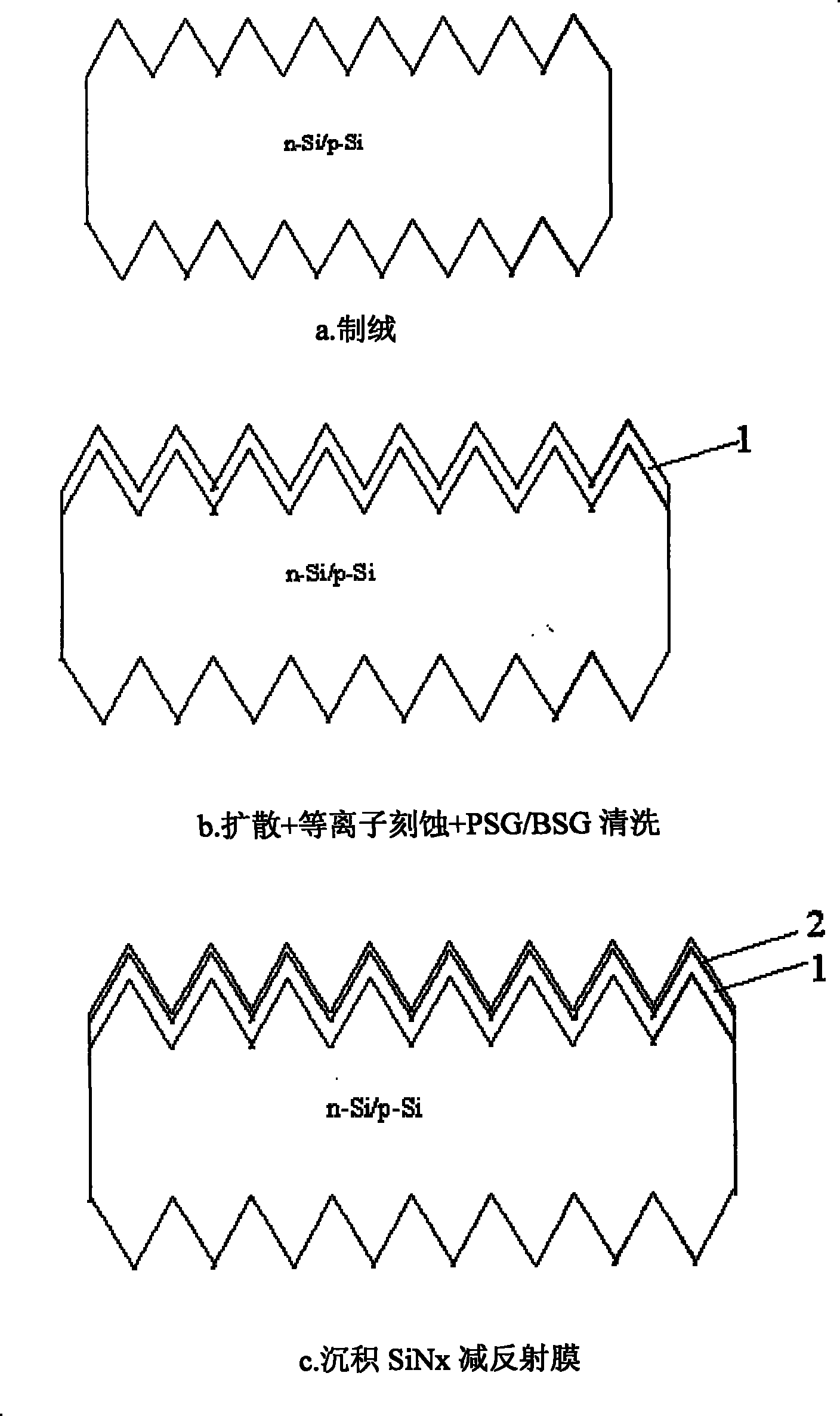
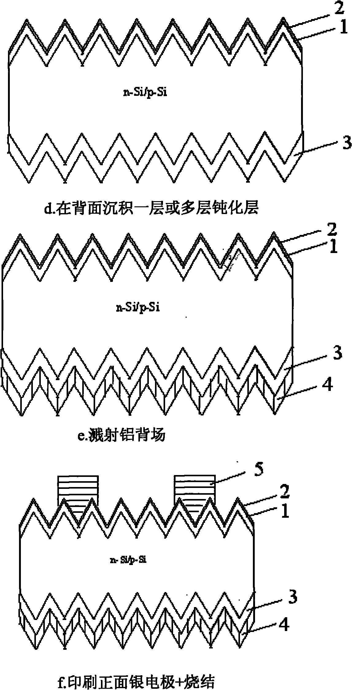
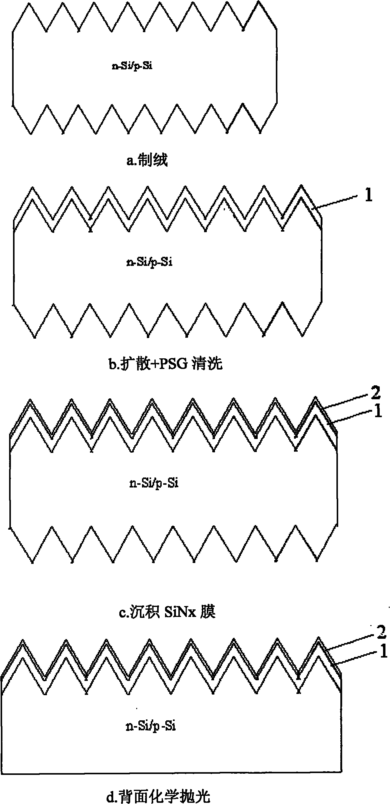
[0043] The method for preparing a solar cell using a local back field provided in this example is as follows: first select an N-type or P-type silicon wafer for texturing, then perform boron or phosphorus diffusion on the N-type silicon wafer, and perform phosphorus diffusion on the P-type silicon wafer After cleaning the borosilicate glass or phosphosilicate glass layer remaining on the surface of the silicon wafer after diffusion, the silicon nitride film is deposited on the front side of the silicon wafer by PECVD, and then the back side is polished by hot lye, and a passivation film is deposited on the polished back side. Thin film, laser opening and sputtering aluminum layer, and finally silver electrode screen printing on the front of the silicon wafer, sintering and test sorting.
[0044] The lye used for back polishing is inorganic lye, the inorganic lye is sodium hydroxide or potassium hydroxide aqueous solution, its weight percentage is 5-50%, and the temperature is 5...
Embodiment 2
[0047] The method for preparing a solar cell using a localized back field provided in this embodiment includes the following steps:
[0048] (1) Wafer selection, texturing and cleaning
[0049] Select N-type monocrystalline silicon wafers, use 0.5-3% by weight sodium hydroxide aqueous solution to make texture to obtain pyramid-shaped texture, and then wash off the lye;
[0050] (2) Diffusion doping of phosphorus or boron
[0051] For N-type silicon wafers, the boron tribromide liquid source is used to diffuse, and the boron source diffuses into the silicon wafer after diffusion;
[0052] (3) Removal of borosilicate glass
[0053] Immersing the diffused silicon wafer in hydrofluoric acid with a volume percentage of 5-15% to clean away the borosilicate glass remaining on the surface of the silicon wafer;
[0054] (4) SiNx film deposition
[0055] The silicon wafer cleaned with borosilicate glass is deposited on the front side of the silicon nitride film by PECVD;
[0056] (...
Embodiment 3
[0066] The method for preparing a solar cell using a localized back field provided in this embodiment includes the following steps:
[0067] (1) Wafer selection, texturing and cleaning
[0068] Select P-type monocrystalline silicon wafers, use 0.5-3% by weight sodium hydroxide aqueous solution to make texture to obtain pyramid-shaped texture, and then wash off the lye;
[0069] (2) Diffusion doping of phosphorus or boron
[0070] For P-type silicon wafers, phosphorus oxychloride liquid source is used to diffuse, and the phosphorus source diffuses into the silicon wafer after diffusion;
[0071] (3) Removal of phosphosilicate glass
[0072] Immersing the diffused silicon wafer in hydrofluoric acid with a volume percentage of 5-15% to wash off the phosphosilicate glass remaining on the surface of the silicon wafer;
[0073] (4) SiNx film deposition
[0074] Deposit silicon nitride film on the front side of the silicon wafer cleaned with phospho-silicate glass by PECVD;
[0...
PUM
 Abstract
Description
Claims
Application Information


