Solar cell

A solar cell and electrode technology, applied in the field of solar cells, can solve the problems of thermal mismatch, lattice mismatch between gallium nitride epitaxial layer and silicon substrate, etc., achieve high absorption rate, reduce process cost and equipment depreciation cost, Simple preparation process

Inactive Publication Date: 2010-10-20
HUAZHONG UNIV OF SCI & TECH
View PDF4 Cites 22 Cited by
  • Summary
  • Abstract
  • Description
  • Claims
  • Application Information

AI Technical Summary

Problems solved by technology

The biggest technical problem at present is that there is a huge lattice mismatch and thermal mismatch between the GaN epitaxial layer and the silicon substrate, and it is easy to form amorphous silicon nitride during the growth of the GaN film (see literature: Jiang Fengyi , progress in research and development of gallium nitride LED materials and devices on silicon substrates. Abstracts of the 11th National Luminescence Academic Conference, 2007.), so if you want to obtain high-quality gallium nitride materials on silicon substrates without cracks , it is necessary to find a suitable buffer layer material and optimize the epitaxial process to solve these problems

Method used


Image

  • Solar cell
  • Solar cell

Examples


Embodiment 1

[0019] Embodiment 1: a silicon-based single-junction indium gallium nitride (InGaN) solar cell.

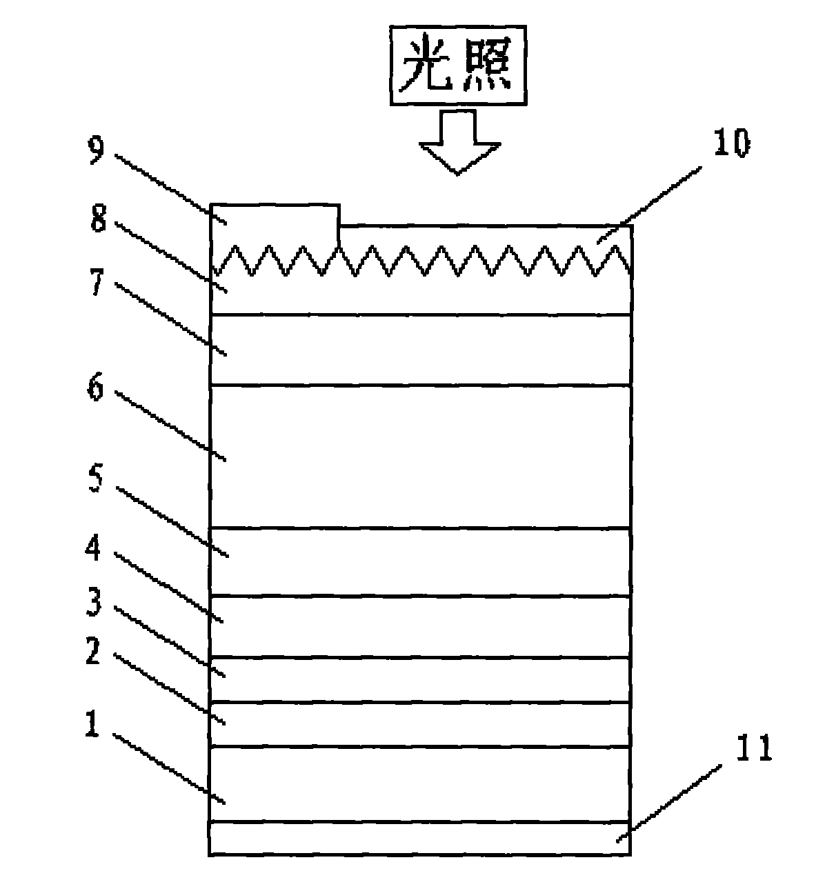
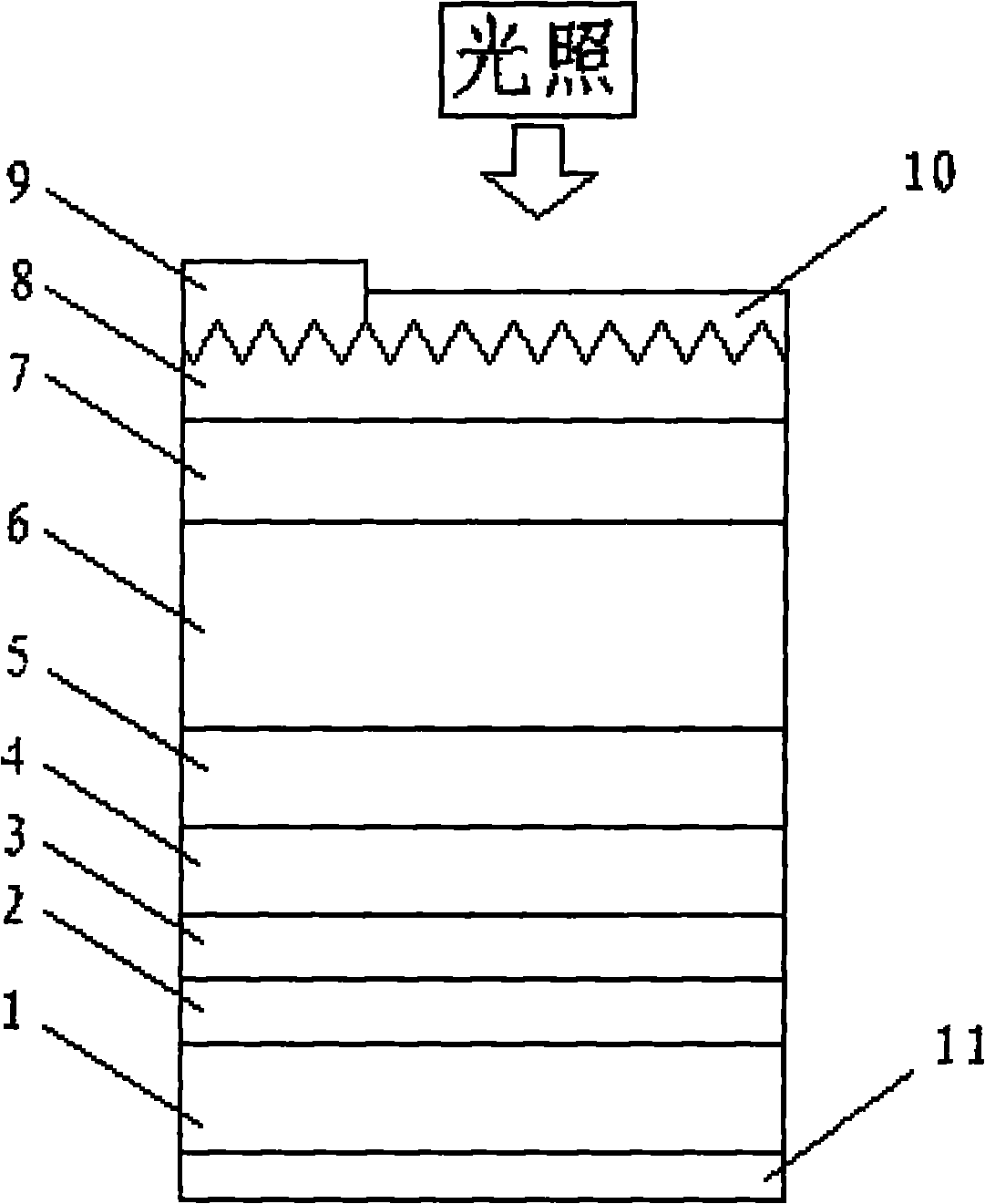
[0020] The structure of the solar cell is as figure 1 As shown: an n-type doped silicon substrate 1 is provided, and a layer of zinc oxide seed crystal layer 2 is formed on the silicon substrate. A zinc oxide nano-array buffer layer 3 is provided, which is fabricated on the zinc oxide seed crystal layer 2 . A layer of n-type doped gallium nitride buffer layer 4 is provided on the zinc oxide nano-array buffer layer 3 . With a layer of n-type doped In a Ga 1-a The N layer is made on the n-type doped gallium nitride buffer layer 3 . With a layer of unintentionally doped In b Ga 1-b N-layer 6, which is fabricated on n-type doped In a Ga 1-a N layer 5 above. with a layer of p-doped In c Ga 1-c N-layer 7, which is fabricated on unintentionally doped In b Ga 1-b N layer above. There is a layer of p-type heavily doped GaN window layer 8, which is fabricated on p-type doped I...

Embodiment 2

[0032] Example 2: Preparation of a silicon-based single-junction indium gallium nitride (InGaN) solar cell.

[0033] The preparation of the solar cell adopts the method comprising the following steps:

[0034] Step 1: Select an n-type doped silicon substrate 1, and obtain an n-type doped silicon wafer by doping phosphorus impurities;

[0035] Step 2: sputtering a 0.01-0.1 μm thick zinc oxide seed layer 2 on the surface of the silicon substrate, and then growing an aligned zinc oxide nano-array buffer layer 3 on the surface of the silicon wafer by wet chemical method, hydrothermal method or other methods , with a thickness of 0.2-2.5 μm.

[0036] Step 3: growing a silicon-doped n-type gallium nitride buffer layer 4 on the zinc oxide nano-array buffer layer 3 by using metal organic chemical vapor deposition technology. The growth temperature is 1000-1150°C, the growth pressure is 50-500torr, the thickness is 0.5-3μm, and the electron concentration is 1E16-1E19 / cm 3 ;

[0037...


PUM


Abstract

The invention relates to a silicon-based single-junction gallium indium nitride solar cell which comprises a back electrode (11), a silicon substrate (1), a seed crystal layer (2), a buffer layer (3), an n-type doped GaN buffer layer (4), an InaGal-aN layer (5), an unintentional doped InbGal-bN layer (6), a p-type doped IncGal-cN layer (7), a window layer (8), a positive electrode (9) and an anti-reflection conductive film (10) which are arranged from bottom to top, wherein the silicon substrate and the InaGal-aN layer is are an n-type doped structure, the seed crystal layer and the buffer layer are made of ZnO material, the window layer is made of p-type heavily doped GaN, and the anti-reflection conductive film covers areas of the window layer other than the positive electrode. The solar cell can quite effectively solve the problems of lattice matching, thermal expansion coefficient matching and the like encountered when a GaN film extends from the silicon substrate, and has the advantages of low manufacturing cost, high sunlight absorbability and the like.

Description

technical field [0001] The invention relates to a solar cell, in particular to a silicon-based single-junction gallium indium nitride solar cell. Background technique [0002] A solar cell is a photovoltaic device that converts solar energy directly into electrical energy. According to different preparation materials, it is mainly divided into crystalline silicon solar cells, silicon-based thin film solar cells, CIGS (copper indium gallium tin) solar cells, III-V solar cells represented by gallium arsenide, organic polymer solar cells, etc. . The first four types of solar cells are semiconductor solar cells, which are currently the most widely used. The principle of semiconductor solar cells is to use the photovoltaic effect of semiconductor pn junctions, that is, to use materials with a certain band gap to absorb solar photon energy to excite electron-hole pairs to generate photoelectromotive force, thereby completing the conversion of light energy to electrical energy. ...

Claims


Application Information

Patent Timeline
Patent Type & Authority Applications(China)
IPC IPC(8): H01L31/042H01L31/0304H01L31/18
CPCY02E10/50Y02P70/50
Inventor 汪连山申志辉刘胜
Owner HUAZHONG UNIV OF SCI & TECH
Why Eureka
Try Eureka