CMOS (Complementary Metal Oxide Semiconductors) semiconductor integrated circuit with high irradiation resistance and preparation method thereof

A technology of integrated circuits and semiconductors, applied in semiconductor/solid-state device manufacturing, circuits, transistors, etc., can solve the problems of wasting active area area, poor resistance and capacitance characteristics, increasing process steps and complexity, and cost, so as to reduce charge Trapping centers, preventing latch-up effects, and reducing device defects

Inactive Publication Date: 2011-01-19
UNIV OF ELECTRONICS SCI & TECH OF CHINA
View PDF4 Cites 8 Cited by
  • Summary
  • Abstract
  • Description
  • Claims
  • Application Information

AI Technical Summary

Problems solved by technology

PN junction isolation requires complex circuit design and produces poor resistance-capacitance characteristics
The lateral dimension of LOCOS isolation technology cannot be precisely controlled, and it is not applicable as the process line width decreases. At the same time, there is a bird's beak phenomenon, which wastes the area of ​​the active area and affects the integration level.
For STI, on the one hand, the total dose irradiation response is worse than LOCOS isolation technology, on the other hand, irradiation will cause leakage current under the shallow trench, which will turn on the parasitic transistor and cause latch-up effect
Although 5Mard (SiO 2 ) level of reinforcement, but increases the steps and complexity and cost of the process

Method used


Image

  • CMOS (Complementary Metal Oxide Semiconductors) semiconductor integrated circuit with high irradiation resistance and preparation method thereof
  • CMOS (Complementary Metal Oxide Semiconductors) semiconductor integrated circuit with high irradiation resistance and preparation method thereof
  • CMOS (Complementary Metal Oxide Semiconductors) semiconductor integrated circuit with high irradiation resistance and preparation method thereof

Examples


Embodiment 1

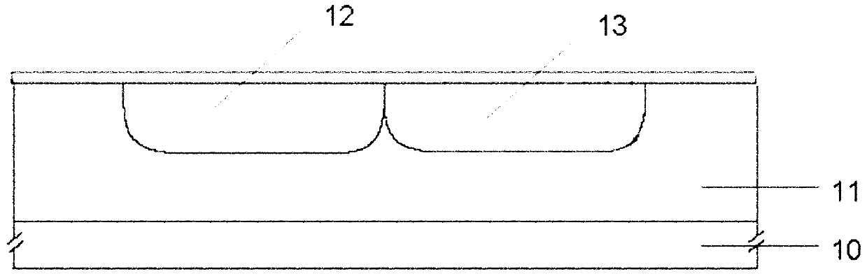
[0032] The substrate is a p-type silicon wafer 10, and a p-epitaxial layer 11 is grown, and the thickness of the p-epitaxial layer 11 is about 5.0 μm. see Figure 4 , forming a double well process, thermally growing on the surface of the p- epitaxial layer 11 with a thickness of about 150 The masking oxide layer is used to protect the surface from contamination and reduce injection damage. The n-well implantation region is photolithographically etched, and phosphorus is implanted to form the n-well 12 , and the p-well implantation region is photolithographically etched, and boron is implanted to form the p-well 13 .

[0033] For deep trench etching see Figure 5 , using hydrofluoric acid to remove the masking oxide layer, and thermally grow a thin oxide layer 20 with a thickness of about 150 As a corrosion protection layer for the source region when the upper silicon nitride film is removed; then use LPCVD to deposit silicon nitride 21 as a barrier layer for chemical mech...

Embodiment 2

[0038] The substrate is a p-type silicon wafer 10, on which a p- epitaxial layer 11 is grown with a thickness of about 5.0 μm. see Figure 4 , forming a double well process, the thermal growth thickness is about 120 The masking oxide layer is used to protect the surface from contamination and reduce implantation damage. The n-well injection region is photolithographically implanted with phosphorus to form the n-well 12, and the p-well implantation region is photolithographically implanted to form the p-well 13.

[0039] For deep trench etching see Figure 5 , use hydrofluoric acid to remove the masking oxide layer, and thermally grow a thin oxide layer 20 with a thickness of about 120 As a corrosion protection layer for the source region when the upper silicon nitride film is removed; then use LPCVD to deposit silicon nitride 21 as a barrier layer for chemical mechanical polishing to protect the active region from over-polishing by CMP; photolithography for deep trench iso...

Embodiment 3

[0044] The substrate is a p-type silicon wafer 10, on which a p- epitaxial layer 11 is grown with a thickness of about 5.0 μm. Then perform deep groove etching, and thermally grow a thin oxide layer 20 with a thickness of about 150 As a corrosion protection layer for the source region when the upper silicon nitride film is removed; then use LPCVD to deposit silicon nitride 21 as a barrier layer for chemical mechanical polishing to protect the active region from over-polishing by CMP; photolithography for deep trench isolation Region 22, and then use DRIE to etch through the entire epitaxial layer to obtain deep grooves. Deep trench oxide filling, thermally grown trench liner silicon oxide 30, thickness about 150 Then HWP is used to fill the trench with silicon oxide 31 .

[0045] Deep trench oxide polishing - nitride removal see Figure 7 , using CMP to polish the trench silicon oxide, and then hot phosphoric acid to remove the silicon nitride.

[0046] A double well pro...


PUM


Abstract

The invention relates to a CMOS (Complementary Metal Oxide Semiconductors) semiconductor integrated circuit with high irradiation resistance and a preparation method thereof, relating to the technical field of integrated circuits. The CMOS semiconductor integrated circuit comprises a substrate (10), an epitaxial layer (11), a p well and an n well, wherein at least one isolation groove (31) is arranged between the p well and the n well and penetrates through the epitaxial layer (11); the bottom end of each isolation groove (31) is arranged on the substrate (10); and insulating mediums are filled in the isolation grooves (31). The invention enhances the combination of base regions of a parasitic bipolar transistor, thereby reducing the gain and also greatly reducing the gain of a loop and then effectively preventing latch-up effect.

Description

technical field [0001] The present invention relates to integrated circuit technology. Background technique [0002] With the development of space technology and nuclear technology, more and more electronic devices need to be applied in various irradiation environments. The amount of radiation that semiconductor integrated circuits receive during work is mainly determined by the radiation environment and its working conditions. Irradiation interacts with components in semiconductor integrated circuits, causing their electrical performance parameters to change or even fail, resulting in the failure of semiconductor integrated circuits, resulting in electronic equipment not working properly. In order to make electronic equipment work normally in a specific radiation environment, it is necessary to improve the radiation resistance of semiconductor integrated circuits. [0003] A Complementary Metal Oxide Semiconductor (CMOS) device is a basic electronic device, and a CMOS int...

Claims


Application Information

Patent Timeline
Patent Type & Authority Applications(China)
IPC IPC(8): H01L27/092H01L21/8238H01L21/762
Inventor 李平李威李建军
Owner UNIV OF ELECTRONICS SCI & TECH OF CHINA
Why Eureka
Try Eureka