Preparation method of crescent nanometer metal structures
A metal nano, crescent-shaped technology, which is applied in the fields of nanostructure manufacturing, nanotechnology, nanotechnology, etc., can solve the difficulty in realizing the controllable preparation of repetitive crescent-shaped metal nanostructures, the size of limited lithography resolution, and the low efficiency. and other problems, to achieve the effect of controllable size and shape, low cost and high efficiency
- Summary
- Abstract
- Description
- Claims
- Application Information
AI Technical Summary
Problems solved by technology
Method used
Image
Examples
Embodiment 1
[0047] A method for preparing a crescent-shaped metal nanodisk array of the present invention, comprising the following steps:
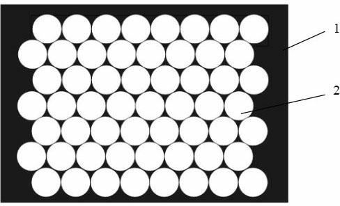
[0048] (1) Preparation of monolayer ordered polystyrene nanosphere dense arrangement:
[0049] a) Prepare the silicon wafer: select a (110) oriented silicon wafer with a size of 25mm×25mm×0.5mm as the substrate 1, and put the silicon wafer into acetone, ethanol, and deionized water for ultrasonic cleaning for 30 minutes, and then put hydrogen peroxide and 98 % concentrated sulfuric acid was heated to 80°C, and the ultrasonically cleaned silicon chips were soaked in it for 1 hour. Soak in the washing solution at ℃ for 1 hour, take it out and rinse it repeatedly to obtain a clean and hydrophilic surface of the silicon wafer, and place it in absolute ethanol for later use;
[0050] b) Preparation of polystyrene nanosphere suspension system: select polystyrene nanospheres with an average particle size of 300 nm and a monodispersity of less than 5%, and ...
Embodiment 2
[0059] A method for preparing a crescent-shaped gold nanodisk structure array supported by silicon pillars of the present invention, comprising the following steps:
[0060]Using the crescent-shaped gold nanodisk array prepared in Example 1 as a mask, in an inductively coupled plasma etching vacuum chamber, using sulfur hexafluoride and argon as gas sources, the The chip is etched, the volume flow rate of sulfur hexafluoride is 50 sccm, the volume flow rate of argon gas is 35 sccm, the vacuum degree of the vacuum chamber is controlled at 0.01±0.003Pa, the RF power during the etching process is 40W, and the etching time is 12min. After the etching is completed, the obtained Figure 14 A crescent-shaped array of gold nanoparticles supported by silicon pillars is shown (substrate 1 forming silicon pillars 8 and gold film forming gold nanoparticles 9).
Embodiment 3
[0062] A method for preparing discrete crescent-shaped gold-silver composite nanoparticles of the present invention, comprising the following steps:
[0063] (1) Prepare a single layer of ordered polystyrene nanospheres densely arranged: select polystyrene nanospheres with an average particle size of 200nm, and the volume ratio of the solvent to the solvent is 25%, the spin-coating speed is 2000rpm, and the spin-coating time is 12min. Other processes are with embodiment 1;
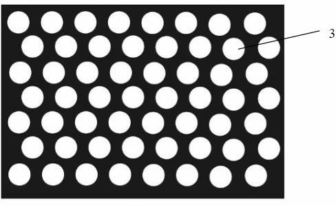
[0064] (2) Prepare a non-dense arrangement of single-layer ordered polystyrene nanospheres: same as Example 1, the difference is that the etching time is 5 min to 7 min;
[0065] (3) deposit chromium: with embodiment 1;
[0066] (4) Preparation of chromium nano-hole array: same as Example 1;
[0067] (5) Prepare a crescent-shaped mask hole array of composite material: select silica nanospheres with an average particle size of 130 nm (formulate a silica nanosphere suspension system with a volume ratio of ...
PUM
| Property | Measurement | Unit |
|---|---|---|
| particle size | aaaaa | aaaaa |
| particle size | aaaaa | aaaaa |
| particle size | aaaaa | aaaaa |
Abstract
Description
Claims
Application Information


