

Solar cell device and manufacturing method thereof
A technology of solar cells and devices, which is applied in the manufacture of electric solid devices, capacitor parts, semiconductor/solid devices, etc., can solve the problems of low photocurrent density and energy conversion efficiency, and achieve improved photocurrent density and energy conversion efficiency, Simple operation, and the effect of improving absorption and utilization efficiency
- Summary
- Abstract
- Description
- Claims
- Application Information
AI Technical Summary
Problems solved by technology
Method used
Image

Examples
preparation example Construction
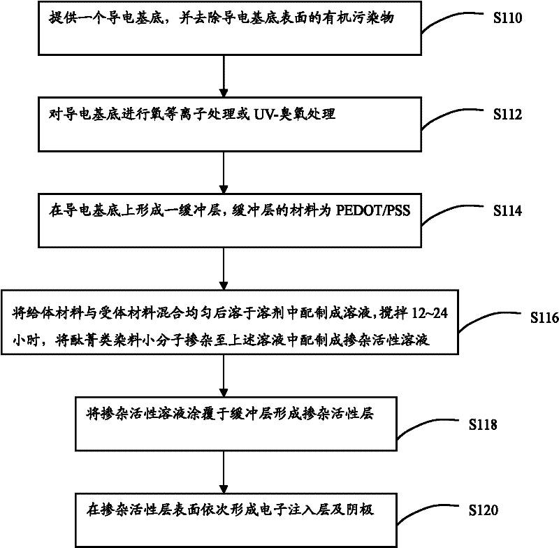
[0030] Please also see figure 2 , the preparation method of the solar cell device of an embodiment, it comprises the following steps;
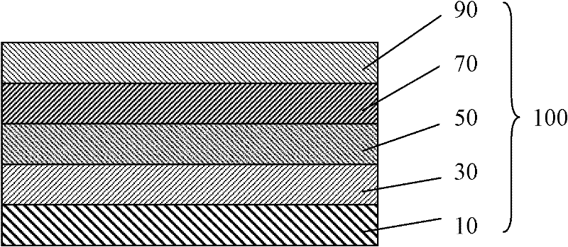
[0031] Step S110 , providing a conductive substrate 10 , and removing organic pollutants on the surface of the conductive substrate 10 . The conductive substrate 10 is indium tin oxide glass (ITO), fluorine doped tin oxide glass (FTO), aluminum doped zinc oxide glass (AZO) or indium doped zinc oxide (IZO) glass. In this embodiment, the conductive substrate 10 is first subjected to photolithography treatment, cut into the required size, and then ultrasonically cleaned with detergent, deionized water, acetone, ethanol, and isopropanone for 15 minutes (min) to remove the conductive substrate 10. Organic contamination of the substrate 10 surface.
[0032] Step S112 , performing oxygen plasma treatment or UV-ozone treatment on the conductive substrate 10 . The oxygen plasma treatment time is 5-15 minutes, and the power is 10-50W; the UV-ozone t...
Embodiment 1
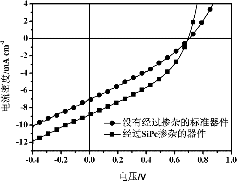
[0041] First mix P3HT and PCBM at a mass ratio of 1:1 to prepare a chlorobenzene solution with a mass concentration of 24 mg / ml, stir well and then add silicon phthalocyanine, the mass concentration of silicon phthalocyanine is 0.5 mg / ml, and stir for 24 hours to form Doping with active solution; then photolithographically process the ITO glass, cut it into the required light-emitting area, and then use detergent, deionized water, acetone, ethanol, and isopropanol to perform ultrasonic cleaning for 15 minutes respectively to remove the surface of the glass. Organic pollutants; after cleaning, oxygen plasma treatment is performed on them, the oxygen plasma treatment time is 5-15min, and the power is 10-50W; after that, the commercially available buffer layer material PEDOT / The PSS solution is spin-coated on the treated substrate, the spin-coating speed is 500-3000rpm, the spin-coating time is 20-60s, the thickness of the buffer layer is 20-80nm, and then baked at 100-200°C for ...
Embodiment 2
[0045] First mix P3HT and PCBM at a mass ratio of 1:1 to prepare a chlorobenzene solution with a mass concentration of 20 mg / ml, stir well and then add silicon phthalocyanine with a mass concentration of silicon phthalocyanine of 0.7 mg / ml, and stir for 24 hours; Then the ITO glass is subjected to photolithography treatment, cut into the required luminous area, and then ultrasonically cleaned with detergent, deionized water, acetone, ethanol, and isopropanol for 15 minutes to remove organic pollutants on the glass surface; After cleaning, it is subjected to oxygen plasma treatment, the oxygen plasma treatment time is 5-15min, and the power is 10-50W; after that, the commercially available buffer layer material PEDOT / PSS solution with a weight ratio of 2:1-6:1 is spin-coated on the On the treated substrate, the spin-coating speed is 500-3000rpm, the spin-coating time is 20-60s, the thickness of the buffer layer is 20-80nm, and then baked at 100-200°C for 15-50min; then transfer ...
PUM
| Property | Measurement | Unit |
|---|---|---|
| thickness | aaaaa | aaaaa |
| thickness | aaaaa | aaaaa |
| current density | aaaaa | aaaaa |
Abstract
Description
Claims
Application Information