Organic semiconductor thin film solar cell preparation method based on nickel oxide anode interface layer

An organic semiconductor and solar cell technology, applied in the manufacture of semiconductor/solid-state devices, semiconductor devices, coatings, etc., can solve the problem of high-power pulsed lasers being expensive, unable to obtain uniform nickel oxide films, and unsatisfactory quality of nickel oxide films, etc. problems, to achieve the effect of high light transmittance, high longevity, compact structure, and improved quality

Inactive Publication Date: 2013-05-22
HEFEI INSTITUTES OF PHYSICAL SCIENCE - CHINESE ACAD OF SCI
View PDF3 Cites 2 Cited by
  • Summary
  • Abstract
  • Description
  • Claims
  • Application Information

AI Technical Summary

Problems solved by technology

Although this solar cell preparation method avoids the defects of producing silicon-based solar cells to a certain extent, it still has the disadvantage that the high-power pulsed laser is expensive, which makes it difficult to reduce the production cost; and the p In the case of a large-area semiconductor layer, due to the uneven distribution of atoms on the surface of the target after vaporization, it is impossible to obtain a large-area uniform nickel oxide film.
At the same time, the surface atomic energy of the target after vaporization is less than 1eV, which also makes the quality of the formed nickel oxide film unsatisfactory.

Method used


Image

  • Organic semiconductor thin film solar cell preparation method based on nickel oxide anode interface layer
  • Organic semiconductor thin film solar cell preparation method based on nickel oxide anode interface layer
  • Organic semiconductor thin film solar cell preparation method based on nickel oxide anode interface layer

Examples


Embodiment 1

[0019] The concrete steps of preparation are:

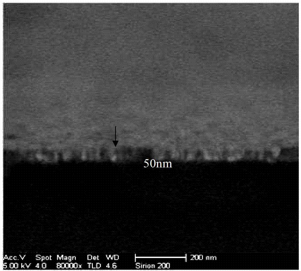
[0020] In step 1, the transparent conductive substrate is ultrasonically cleaned with acetone, ethanol and deionized water, and then blown dry with nitrogen; wherein, the transparent conductive substrate is a conductive film. Then place the nickel oxide bulk target and the transparent conductive substrate on the cathode and the sample stage in the vacuum chamber of the radio frequency magnetron sputtering equipment respectively; wherein, the distance between the nickel oxide bulk target and the transparent conductive substrate is 8cm. The vacuum degree of the vacuum chamber is ≤1×10 -4 After Pa, the vacuum chamber was placed in an argon atmosphere with a pressure of 5Pa, and sputtered for 5min; wherein, the sputtering power was 150W, and the surface covered with figure 1 The nickel oxide film is shown as a transparent conductive substrate.

[0021] Step 2, first mix poly(3-hexylthiophene), [6,6]-phenyl-C 61 -Methyl butyrate an...

Embodiment 2

[0024] The concrete steps of preparation are:

[0025] In step 1, the transparent conductive substrate is ultrasonically cleaned with acetone, ethanol and deionized water, and then blown dry with nitrogen; wherein, the transparent conductive substrate is a conductive film. Then place the nickel oxide bulk target and the transparent conductive substrate on the cathode and the sample stage in the vacuum chamber of the radio frequency magnetron sputtering equipment respectively; wherein, the distance between the nickel oxide bulk target and the transparent conductive substrate is 9 cm. The vacuum degree of the vacuum chamber is ≤1×10 -4 After Pa, the vacuum chamber was placed in an argon atmosphere with a pressure of 4 Pa, and sputtered for 11 minutes; wherein, the sputtering power was 138W, and the surface covered with figure 1 The nickel oxide film is shown as a transparent conductive substrate.

[0026] Step 2, first according to the weight ratio of 0.95:0.85:99, poly(3-hexy...

Embodiment 3

[0029] The concrete steps of preparation are:

[0030] In step 1, the transparent conductive substrate is ultrasonically cleaned with acetone, ethanol and deionized water, and then blown dry with nitrogen; wherein, the transparent conductive substrate is a conductive film. Then place the nickel oxide bulk target and the transparent conductive substrate on the cathode and the sample stage in the vacuum chamber of the radio frequency magnetron sputtering equipment respectively; wherein, the distance between the nickel oxide bulk target and the transparent conductive substrate is 10 cm. The vacuum degree of the vacuum chamber is ≤1×10 -4 After Pa, the vacuum chamber was placed under an argon atmosphere with a pressure of 3 Pa, and sputtered for 17 minutes; wherein, the sputtering power was 125W, and the surface covered with figure 1 The nickel oxide film is shown as a transparent conductive substrate.

[0031] Step 2, first mix poly(3-hexylthiophene), [6,6]-phenyl-C 61 -Methyl...


PUM

PropertyMeasurementUnit
thicknessaaaaaaaaaa
thicknessaaaaaaaaaa
optical band gapaaaaaaaaaa

Abstract

The invention discloses an organic semiconductor thin film solar cell preparation method based on a nickel oxide anode interface layer. The organic semiconductor thin film solar cell preparation method includes: placing nickel oxide block target materials and a transparent conductive substrate into a radio frequency magnetron sputtering device; sputtering in an argon atmosphere or an argon and oxygen mix atmosphere so as to obtain a transparent conductive substrate covered with nickel oxide film; then, mixing poly (3-hexylthiophene), [6,6]- phenyl-C61-methyl butyrate and chlorobenzene in an inert atmosphere, and stirring to obtain photosensitive coatings; coating the transparent conductive substrate covered with the nickel oxide film with the photosensitive coatings under the inert atmosphere; performing annealing treatment on the transparent conductive substrate so as to obtain a transparent conductive substrate covered with the nickel oxide film and photosensitive film in sequence; furthermore, using an electron beam evaporation method for lithium fluoride film and aluminum film evaporation on the surface of the transparent conductive substrate covered with the nickel oxide film and the photosensitive film in sequence; and finally, placing the transparent conductive substrate in the inert atmosphere to complete encapsulating and accordingly obtaining a target product. According to the organic semiconductor thin film solar cell preparation method based on the nickel oxide anode interface layer, production cost is low, and the nickel oxide film is large in area and good in quality.

Description

technical field [0001] The invention relates to a method for preparing a solar cell, in particular to a method for preparing an organic semiconductor thin film solar cell based on a nickel oxide anode interface layer. Background technique [0002] At present, the development and utilization of solar energy is one of the effective means to solve the energy crisis in the world. The main way is to directly convert solar energy into electrical energy through the photovoltaic effect. The silicon-based solar cells that realize this conversion process have entered the stage of industrial production and commercial application, but the further development of its application is limited due to the high production cost and high energy consumption of conversion devices, and the defects such as heavy metal pollution. For this reason, in order to solve this problem, people have made unremitting efforts, such as the Chinese invention patent application CN 101836307 A published on September ...

Claims


Application Information

Patent Timeline
Patent Type & Authority Applications(China)
IPC IPC(8): H01L51/48C23C14/30C23C14/06C23C14/18C23C14/35C23C14/08
CPCY02E10/549Y02P70/50
Inventor 曾雪松史同飞肖正国李宁王玉琦
Owner HEFEI INSTITUTES OF PHYSICAL SCIENCE - CHINESE ACAD OF SCI
Why Eureka
Try Eureka