Self-aligned double-layer channel metallic oxide thin film transistor and manufacturing method thereof

An oxide film and transistor technology, applied in semiconductor/solid-state device manufacturing, semiconductor devices, electrical components, etc., can solve the problem of not being able to meet the requirements of data circuit driving, affecting device reliability and power consumption, and device off-state current change. Large and other problems, to reduce parasitic capacitance, achieve self-alignment, high on-state current effect

Active Publication Date: 2013-10-09
PEKING UNIV SHENZHEN GRADUATE SCHOOL
View PDF3 Cites 13 Cited by
  • Summary
  • Abstract
  • Description
  • Claims
  • Application Information

AI Technical Summary

Problems solved by technology

[0005] Compared with the bottom gate structure device, the top gate structure is easy to achieve self-alignment, but the source and drain region resistance of the self-aligned top gate structure device has a great influence on the device performance. In the large-area panel production line, the low-resistance source-drain compatible with it The formation process is extremely important; moreover, top-gate structure devices are greatly affected by ambient light, and the off-

Method used


Image

  • Self-aligned double-layer channel metallic oxide thin film transistor and manufacturing method thereof
  • Self-aligned double-layer channel metallic oxide thin film transistor and manufacturing method thereof
  • Self-aligned double-layer channel metallic oxide thin film transistor and manufacturing method thereof

Examples


Embodiment 1

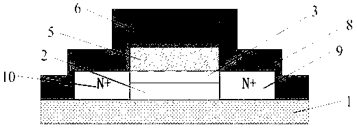
[0067] A specific example of the manufacturing method of the thin film transistor of the present invention is as follows Figure 1 to Figure 7 shown, including the following steps:

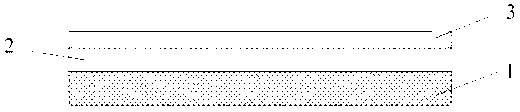
[0068] Such as figure 1 As shown, the substrate 1 used is a glass substrate or a flexible substrate, and a 60nm high-resistivity metal oxide semiconductor indium gallium zinc oxide (IGZO) film 2 is grown on the substrate by magnetron sputtering; A 5nm low-resistivity indium tin oxide film (ITO)3 was grown by sputtering.

[0069] Such as figure 2 As shown, the photoresist 4 is spin-coated, and the indium tin oxide and indium gallium zinc oxide thin films are photolithographically and etched; the photoresist 4 is removed by ultrasonication with acetone.

[0070] Such as image 3 As shown, on the low-resistivity indium tin oxide film 3, a layer of 200nm silicon oxide film 5 (that is, the gate dielectric layer) is deposited by plasma enhanced chemical vapor deposition (PECVD); then magnetron spu...

Embodiment 2

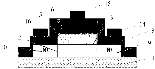
[0076] Another specific example of the manufacturing method of the thin film transistor of the present invention is as follows Figure 8 to Figure 14 shown, including the following steps:

[0077] Such as Figure 8 As shown, the substrate 1 used is a glass substrate, and a layer of 80nm high-resistivity metal oxide semiconductor indium gallium zinc oxide (IGZO) film 2 is grown on the substrate by magnetron sputtering; and then grown by magnetron sputtering A 15nm low-resistivity indium tin oxide film (ITO)3.

[0078] Such as Figure 9 As shown, the photoresist 4 is spin-coated, and the indium tin oxide and indium gallium zinc oxide thin films are photolithographically and etched; the photoresist 4 is removed by ultrasonication with acetone.

[0079] Such as Figure 10 As shown, a 300nm silicon oxide film 5 is deposited on the low-resistivity indium tin oxide film 3 by plasma enhanced chemical vapor deposition (PECVD); then a 300nm metal layer is grown by magnetron sputteri...

Embodiment 3

[0085] Another specific example of the manufacturing method of the thin film transistor of the present invention is as follows Figure 15 to Figure 22 shown, including the following steps:

[0086] Such as Figure 15 As shown, the substrate 1 used is a flexible substrate, and a layer of 100nm SiO is grown on the substrate 1 by plasma enhanced chemical vapor deposition (PECVD). 2 buffer layer 17.

[0087] Such as Figure 16 As shown, a layer of 40nm high-resistivity metal oxide semiconductor indium gallium zinc oxide (IGZO) film 2 is grown by magnetron sputtering on the substrate deposited with a buffer layer; then a layer of 5nm is grown by magnetron sputtering low-resistivity indium tin oxide (ITO) films 3 .

[0088] Such as Figure 17 As shown, the photoresist 4 is spin-coated, and the indium tin oxide and indium gallium zinc oxide thin films are photolithographically and etched; the photoresist 4 is removed by ultrasonication with acetone.

[0089] Such as Figure 18...


PUM

PropertyMeasurementUnit
Thicknessaaaaaaaaaa
Thicknessaaaaaaaaaa
Thicknessaaaaaaaaaa

Abstract

The invention provides a self-aligned double-layer channel metallic oxide thin film transistor and a manufacturing method of the self-aligned double-layer channel metallic oxide thin film transistor. The manufacturing method comprises the following steps that a thick high-resistivity metallic oxide semiconductor layer and a thin low-resistivity metallic oxide layer deposit on a substrate, so that double layers of channels are formed; photoetching and etching are carried out on the double layers of channels, so that an active area graph is formed; a gate medium layer and a gate electrode are formed on the double layers of channels; a covering layer with H deposits on the whole substrate, then heat processing is carried out so that H can diffuse to metallic oxide outside the channel area not covered by the gate electrode and the gate medium, and a heavily doped low-resistivity source drain area is formed; a contact hole and a contact electrode are prepared. The self-aligned double-layer channel metallic oxide thin film transistor and the manufacturing method of the self-aligned double-layer channel metallic oxide thin film transistor adopt self-aligned double-layer channel top gate structure, can lower source drain resistance, lower the influence of ambient light on elements, lower off-state current, and improve on-state current and migration rate of the elements.

Description

technical field [0001] The invention relates to a thin film transistor and a preparation method thereof, in particular to a self-aligned top gate structure double-layer channel metal oxide thin film transistor and a preparation method thereof. Background technique [0002] Thin-film transistors (TFTs: thin-film transistors), as a kind of MOS device, have always been the core device of flat panel display technology. Thin film transistors are mainly used in the switch control of the pixel circuit of the flat panel display panel, the driving of the pixel circuit and the peripheral driving circuit of the display panel. In addition, thin film transistors are also widely used in sensors, memories, processors and other fields. Thin film transistors can be divided into many types according to the different materials of the active layer, including traditional silicon-based thin film transistors, metal oxide thin film transistors (Oxide TFTs) and organic thin film transistors (Organi...

Claims


Application Information

Patent Timeline
IPC IPC(8): H01L21/336H01L29/06
Inventor 张盛东肖祥迟世鹏冷传利邵阳
Owner PEKING UNIV SHENZHEN GRADUATE SCHOOL
Why Eureka
Try Eureka