Method for crystallizing amorphous silicon thin films in multi-cycle rapid thermal annealing auxiliary metal induced mode

An amorphous silicon thin film and auxiliary metal technology, which is applied in the manufacture of semiconductor/solid state devices, electrical components, circuits, etc. Induction, low cost, effect of reducing the amount of residual metal contamination

Inactive Publication Date: 2014-01-01
SHANGHAI UNIV
View PDF5 Cites 3 Cited by
  • Summary
  • Abstract
  • Description
  • Claims
  • Application Information

AI Technical Summary

Problems solved by technology

[0004] Usually the metal layer is prepared by sputtering or evaporation, but these two methods have some fatal defects: the cost of these two technologies

Method used


Image

  • Method for crystallizing amorphous silicon thin films in multi-cycle rapid thermal annealing auxiliary metal induced mode
  • Method for crystallizing amorphous silicon thin films in multi-cycle rapid thermal annealing auxiliary metal induced mode

Examples


Embodiment Construction

[0022] Specific embodiments of the present invention will be further described as follows in conjunction with the accompanying drawings.

[0023] The process and steps in the embodiment of the present invention are as follows:

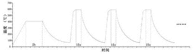
[0024] 1) Cut a common glass slide into a size of 1cm×1cm, ultrasonically clean the surface of the sample with acetone, ethanol and deionized water respectively, and then dry it with nitrogen. Put the cleaned glass substrate into the film deposition chamber, and use plasma enhanced chemical vapor deposition (PECVD) equipment to deposit a layer of amorphous silicon (a-Si) film on the glass substrate with a thickness of about 200nm. When the substrate temperature is 200°C, the deposition pressure is 10 -5 Pa, gas glow pressure range 50Pa~250Pa, RF power supply 13.56MHz, gas source is 100% pure silane (SiH 4 ), hydrogen used as dilute silane (H 2 ) with a purity of 5N.

[0025] 2) Prepare ethanol and toluene solution (volume ratio 1:4), add ethyl cell...


PUM


Abstract

The invention relates to a method for crystallizing amorphous silicon thin films in a multi-cycle rapid thermal annealing auxiliary metal induced mode, and belongs to the technical field of polycrystalline silicon thin film preparation processes. The amorphous silicon thin films are deposited on a glass slide substrate with a vapour deposition method; nickel chloride is dissolved into mixed solution of ethyl alcohol and toluene, and ethyl cellulose is added in to form a viscid and thick solution; spinning coating is performed on the solution, and then annealing is performed on the solution at 400 DEG C for two hours; then rapid thermal annealing processing is performed, the temperature rising rate is about 150-200 DEG C/s, temperature of thin film samples is raised to about 600 DEG C from the room temperature, the 600 DEG C is kept for 15s, then natural cooling is performed, and next-time rapid thermal annealing processing is performed after the temperature of the thin films is lowered to the room temperature; the amorphous silicon thin films can be crystallized after three times of rapid thermal annealing. Compared with a traditional solid-phase crystallizing method and a conventional metal induced crystallizing method, the method has the advantages that annealing temperature is lowered, residual metal pollutant amount is reduced, the annealing time is shortened, and the method is simple in process and low in cost.

Description

technical field [0001] The invention relates to a method for multi-cycle rapid thermal annealing assisting metal-induced crystallization of an amorphous silicon film, belonging to the technical field of polysilicon film preparation. Background technique [0002] Polycrystalline silicon thin film has high carrier mobility, light absorption rate and stable photoelectric performance, so it is widely used in a variety of electronic devices, such as thin film transistors (TFT), image sensors, solar cells, etc., and has been adopted by the photovoltaic industry. It is generally recognized as a candidate for second-generation solar cells with high efficiency, low cost, and long life. Generally, high-quality polysilicon films with large grains help to improve the conversion efficiency of polysilicon thin film solar cells. [0003] At present, the methods for preparing polysilicon thin films mainly include chemical vapor deposition (CVD), solid phase crystallization (SPC), laser crys...

Claims


Application Information

Patent Timeline
IPC IPC(8): H01L21/02
CPCH01L21/02422H01L21/02532H01L21/02672
Inventor 金晶戴文韫瞿晓雷邱宇峰史伟民
Owner SHANGHAI UNIV
Why Eureka
Try Eureka